eBook - ePub
Semiconductor Nanomaterials for Flexible Technologies
From Photovoltaics and Electronics to Sensors and Energy Storage
- 320 pages
- English
- ePUB (mobile friendly)
- Available on iOS & Android
eBook - ePub
Semiconductor Nanomaterials for Flexible Technologies
From Photovoltaics and Electronics to Sensors and Energy Storage
About this book
This book is an overview of the strategies to generate high-quality films of one-dimensional semiconductor nanostructures on flexible substrates (e.g., plastics) and the use of them as building blocks to fabricating flexible devices (including electronics, optoelectronics, sensors, power systems). In addition to engineering aspects, the physics and chemistry behind the fabrication and device operation will also be discussed as well. Internationally recognized scientists from academia, national laboratories, and industries, who are the leading researchers in the emerging areas, are contributing exceptional chapters according to their cutting-edge research results and expertise. This book will be an on-time addition to the literature in nanoscience and engineering. It will be suitable for graduate students and researchers as a useful reference to stimulate their research interest as well as facilitate their research in nanoscience and engineering.
- Considers the physics and chemistry behind fabrication and device operation
- Discusses applications to electronics, optoelectronics, sensors and power systems
- Examines existing technologies and investigates emerging trends
Trusted by 375,005 students
Access to over 1.5 million titles for a fair monthly price.
Study more efficiently using our study tools.
Information
CHAPTER 1
Flexible Organic Single-
Crystal Field-Effect
Transistors
Polymer Science and Engineering, University of Massachusetts, Amherst, USA
CONTENTS
Introduction
Macroscopic organic single crystals
Micropatterned organic single crystals
Organic single-crystal nanowires
Conclusion
References
INTRODUCTION
The majority of research on flexible electronics has been focused on polycrystalline organic thin films [1, 2], carbon nanotubes [3, 4] and inorganic structures [5]. Much less work has been accomplished in determining the limits of flexibility of organic single-crystal transistors [6, 7]. Organic single crystals have been limited to fundamental charge-transport studies and for determining the performance limitation of organic semiconductors [8–10]. Their high mobilities and outstanding electrical characteristics would make them promising candidates for electronic applications such as drivers for active matrix displays and sensor arrays. However, poor mechanical properties of bulk crystals and low throughput in device fabrication have prevented their use in flexible electronics and other wide-ranging applications. Thus, there is a strong need for the development of mechanically flexible, non-destructive, single-crystal devices with prospective applications in flexible electronics while maintaining the intrinsic properties and characteristics of organic single crystals. Our interest lies in both the fundamental aspect of device mechanics [11] and the practical applications of flexible organic single crystals.
In this chapter strategies for fabricating unconventional organic single crystals on mechanically flexible substrates are reviewed. Figure 1.1 shows a schematic of a flexible transistor test structure. The design shows a three-terminal device fabricated from a flexible substrate [either Kapton or transparent polyethylene terephthalate (PET)], a backside gate evaporated from gold, a dielectric insulating layer spun from poly-4-vinylphenol (PVP), top-contact source-drain electrodes evaporated from gold and the semiconductor single-crystal active layer. The distance between the source and drain electrode is referred to as the channel length (L), while the perpendicular distance is referred to as the channel width (W). Applying a voltage to the gate electrode will form a conductive region at the insulator–semiconductor interface. A second voltage applied to the drain electrode will collect the mobile charges and enable the device to generate current across the source–drain. The effective mobility of the semiconductor can be calculated from the saturation regime using the equation IDS = (W · C · μ/2 · L)(VG – VT) [2], where L is the channel length, W is the channel width, C is the capacitance per unit area of the insulating layer, VT is the threshold voltage, VG is the gate voltage, and μ is the field-effect mobility.
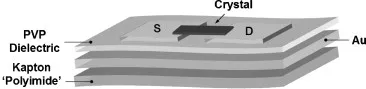
FIGURE 1.1 Schematic of a bottom-contact flexible organic single-crystal field-effect transistor. S: source; D: drain.
This chapter will specifically focus on three classes of flexible organic single-crystal structures: (1) ultrathin macroscopic single crystals, (2) micropatterned single crystals, and (3) single-crystal nanowires. Figure 1.2 shows optical photographs of three representative single-crystal transistors fabricated from the three respective crystal forms. First, the use of field-effect transistors fabricated from ultrathin and conformable macroscopic organic single crystals is described [7, 13]. The use of ultrathin single crystals serves as a proof-of-concept for ‘flexible’ organic single-crystal field-effect transistors with performances exceeding those of previously reported organic thin-film flexible devices. In the second class of single-crystal structures, large-area patterning of organic single crystals onto plastic substrates is reviewed [6, 14–16]. This method is materials-general and yields single-crystal mobilities approaching those of amorphous silicon (Si). Finally, organic single-crystal nanowires are discussed and their use in flexible transistors is demonstrated [12]. The chapter concludes with some perspectives on future research opportunities in the area of flexible organic single-crystal transistors.
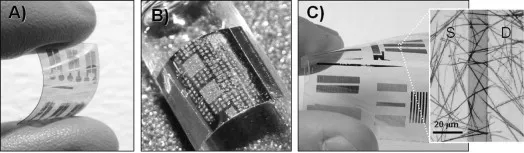
FIGURE 1.2 Representative photographs of (A) ultrathin, (B) micropatterned, and (C) single-crystal nanowire flexible transistors.
(Reprinted with permission from [7] © 2006 Wiley-VCH, [6] © 2006 NPG, and [12] © 2007 American Chemical Society.)
(Reprinted with permission from [7] © 2006 Wiley-VCH, [6] © 2006 NPG, and [12] © 2007 American Chemical Society.)
MACROSCOPIC ORGANIC SINGLE CRYSTALS
Growth via physical vapor transport
The current benchmark for studying charge transport in organic semiconductors is by field-effect transistor experiments with ultrapure organic molecular crystals [8–10]. This is because one can investigate charge transport in the bulk crystal and not be concerned about the static disorder or grain boundaries that typically plague thin films produced via solution-processed methods (i.e. polymers) or thermal evaporation (organic thin films). Unfortunately, disorder in thin films affects the electrical properties of organic semiconductors and, as a result, they are not suitable for determining the performance limits, and more importantly, the intrinsic transport properties of organic semiconductors (Figure 1.3). Although several decades of intensive research have been conducted with single crystals, it was Podzorov et al. who revived their use in field-effect transistors with the high-performance organic semiconductor, rubrene [17]. Over the past five years, a tremendous amount of work has been published with regard to high-mobility single-crystal transistors. Several reviews document their advances, the current status and future outlook [9, 10]. However, one of the major impediments or drawbacks of their use is the fragility and difficulty of mass-producing devices over large areas. Because the fabrication efficiency is slow and tedious, only basic measurements and intrinsic transport phenomena can be conducted with single-crystal transistors. The highest quality organic single crystals are grown via physical vapor transport, a technique that has been employed for well over a century [18]. Figure 1.4 shows a schematic of a furnace tube used to grow high-quality organic single crystals [19]. The same figure shows representative organic single crystal grown via physical transport. Such an instrument can be easily constructed with low-cost parts [18]. Crystals grown from the vapor phase have well-defined faces and smooth crystal surfaces. Slow growth, with a minimum of growth-nucleation sites on the inner walls of the glass cylinders, is a suitable choice to grow thick crystals at growth times of 6–24 h and sublimation temperatures of ∼280–300°C [7]. Typical flow rates used are 50 ml/min. A comprehensive analysis on crystal growth conditions can be found in a previous literature paper [18].
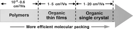
FIGURE 1.3 Current status of organic field-effect transistors. Among the three classes of materials (polymers, thin films and single crystals), organic single crystals dominate the performance of field-effect transistors due to molecular perfection in the crystal lattice. Recent developments in each of the respective areas have produced significant breakthroughs for overcoming the drawbacks in each of the categories (i.e. new highmobility polymers, solution-processable small molecules and patterning techniques).
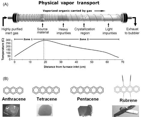
FIGURE 1.4 (A) Physical vapor transport method for growth of single crystals [19]. The source material is placed in the hottest zone of the furnace tube where it sublimes and is carried down a temperature gradient by a stream of inert carrier gas, such as argon. The material resublimes in the cooler zone of the furnace to form large single crystals that can subsequently be hand-picked or patterned onto substrates for fabrication of single-crystal transistors. (B) Examples of oligoacene crystals grown via physical vapor transport. (Reprinted with permission from [19] © 2007 Elsevier, [9] © 2004 Wiley-VCH.)
Growth of ultrathin single crystals
Ultrathin organic single crystals of rubrene are grown by horizontal physical vapor transport growth. Rapid crystal growth results in very thin, large and flat crystal flakes with a transparent appearance (20 min to 1 h growth time). For these results, an initial sublimation temperature of ∼280–300 °C is administered. At the moment nucleation is first observed on the inner glass cylinders, the temperature is increased to ∼330 °C while the argon flow rate is increased from 50 to 100 ml/min. It should be noted that specific parameters may vary from instrument to instrument, but the principle of rapid crystal growth remains the same. These growth conditions enable rubrene single crystals to grow as thin as 100 nm and as large as 1 × 1 cm in size (this is at least 500 times thinner than the standard-grown rubrene crystals). A close analysis of the thin, conformable single crystals shows a nearly defect-free surface morphology. Figure 1.5(A) shows an atom force microscope (AFM) image of the surface morphology of a thin rubrene single crystal. Thin single crystals (i.e. 100 nm to 1 μm) have smaller and less frequent surface steps than thicker crystals. A surface scan over a 2 μm2 area at random locations on different individual samples yielded only one surface step. The surface roughness of a 300 nm thin rubrene single crystal is 0.23 nm, indicating that the surface of the crystal is smooth and free of grain boundaries. A surface island is observed with a monolayer step height of ∼15 Å as shown in the inset, consistent with reported observations [20]. However, a scan of thicker crystals (> 3 μm) showed more frequent and much larger surface steps with a surface roughness of at least twice that of thin crystals (Figure 1.5B). Figure 1.6(A) shows scanning electron microscope (SEM) images of ultrathin rubrene single crystals electrostatically adhered to a device test structure. A high degree of interfacial adhesion and surface conformity is observed with thin crystals compared to thicker crystals (Figure 1.6B). The thick crystal in Figure 1.6(B) shows poor interfacial adhesion and surface brittleness. Field-effect experiments were carried out to monitor the effective mobility at various crystal thicknesses. Results from Figure 1.7 show that mobility gradually drops as a function of crystal thickness. For crystals thicker than 5 μm, the mobility is less than 10–1 cm2/V·s. Excellent adhesion and conformability of thin crystals to the dielectric surface is likely the reason for higher carrier mobility as opposed to the poor crystal–dielectric interface with thicker crystals (as observed in Fig...
Table of contents
- Cover
- Copyright
- Contact Information
- Preface
- Acknowledgment
- Chapter 1 Flexible Organic Single-Crystal Field-Effect Transistors
- Chapter 2 Chemically Synthesized Semiconductor Nanowires for High-Performance Electronics and Optoelectronics
- Chapter 3 Fast Flexible Electronics Made from Nanomembranes Derived from High-Quality Wafers
- Chapter 4 Thin Films of Single-Walled Carbon Nanotubes for Flexible Electronic Device Applications
- Chapter 5 Flexible Field Emitters Based on Carbon Nanotubes and Other Materials
- Chapter 6 Flexible Solar Cells Made of Nanowires/Microwires
- Chapter 7 Zinc Oxide Nanowire Arrays on Flexible Substrates: Wet Chemical Growth and Applications in Energy Conversion
- Chapter 8 Flexible Energy Storage Devices Using Nanomaterials
- Chapter 9 Flexible Chemical Sensors
- Chapter 10 Mechanics of Stiff Thin Films of Controlled Wavy Geometry on Compliant Substrates for Stretchable Electronics
- Index
Frequently asked questions
Yes, you can cancel anytime from the Subscription tab in your account settings on the Perlego website. Your subscription will stay active until the end of your current billing period. Learn how to cancel your subscription
No, books cannot be downloaded as external files, such as PDFs, for use outside of Perlego. However, you can download books within the Perlego app for offline reading on mobile or tablet. Learn how to download books offline
Perlego offers two plans: Essential and Complete
- Essential is ideal for learners and professionals who enjoy exploring a wide range of subjects. Access the Essential Library with 800,000+ trusted titles and best-sellers across business, personal growth, and the humanities. Includes unlimited reading time and Standard Read Aloud voice.
- Complete: Perfect for advanced learners and researchers needing full, unrestricted access. Unlock 1.5M+ books across hundreds of subjects, including academic and specialized titles. The Complete Plan also includes advanced features like Premium Read Aloud and Research Assistant.
We are an online textbook subscription service, where you can get access to an entire online library for less than the price of a single book per month. With over 1.5 million books across 990+ topics, we’ve got you covered! Learn about our mission
Look out for the read-aloud symbol on your next book to see if you can listen to it. The read-aloud tool reads text aloud for you, highlighting the text as it is being read. You can pause it, speed it up and slow it down. Learn more about Read Aloud
Yes! You can use the Perlego app on both iOS and Android devices to read anytime, anywhere — even offline. Perfect for commutes or when you’re on the go.
Please note we cannot support devices running on iOS 13 and Android 7 or earlier. Learn more about using the app
Please note we cannot support devices running on iOS 13 and Android 7 or earlier. Learn more about using the app
Yes, you can access Semiconductor Nanomaterials for Flexible Technologies by Yugang Sun,John A. Rogers in PDF and/or ePUB format, as well as other popular books in Technology & Engineering & Electrical Engineering & Telecommunications. We have over 1.5 million books available in our catalogue for you to explore.