eBook - ePub
Nanotechnology for Microelectronics and Optoelectronics
- 304 pages
- English
- ePUB (mobile friendly)
- Available on iOS & Android
eBook - ePub
Nanotechnology for Microelectronics and Optoelectronics
About this book
When solids are reduced to the nanometer scale, they exibit new and exciting behaviours which constitute the basis for a new generation of electronic devices.
Nanotechnology for Microelectronics and Optoelectronics outlines in detail the fundamental solid-state physics concepts that explain the new properties of matter caused by this reduction of solids to the nanometer scale. Applications of these electronic properties is also explored, helping students and researchers to appreciate the current status and future potential of nanotechnology as applied to the electronics industry.
- Explains the behavioural changes which occur in solids at the nanoscale, making them the basis of a new generation of electronic devices
- Laid out in text-reference style: a cohesive and specialised introduction to the fundamentals of nanoelectronics and nanophotonics for students and researchers alike
Trusted by 375,005 students
Access to over 1.5 million titles for a fair monthly price.
Study more efficiently using our study tools.
Information
Chapter 1
Mesoscopic Physics and Nanotechnologies
1.1 Outlook of the book
1.2 Trends in nanoelectronics and optoelectronics
1.3 Characteristic lengths in mesoscopic systems
1.4 Quantum mechanical coherence
1.5 Quantum wells, wires, and dots
1.6 Density of states and dimensionality
1.7 Semiconductor heterostructures
1.8 Quantum transport
References
Further Reading
Problems
1.1 OUTLOOK OF THE BOOK
The interest in the study of the physical properties of electronic materials of very small sizes, usually in the nanometre range, resides in various factors. One of them is due to the trends in microelectronic integrated devices, for which smaller sizes imply operation at higher frequencies, higher functionality, lower fabrication costs for a given performance, etc. A second reason, more important from a scientific point of view, is related to the appearance of new fundamental physical effects, such as resonant tunnelling, quantum conductance, Coulomb blockade, Hall quantum effects, etc. In addition, very frequently, these fundamental discoveries are related to practical devices like quantum well lasers, single electron transistors, confined quantum Stark effect optical modulators, etc.
In Chapter 1 of this book, we start by reviewing the present trends of microelectronic and optoelectronic semiconductor devices, which are the basis for the new field of nanoelectronics. After this we will revise a series of concepts of mesoscopic physics, such as characteristic lengths, needed for the definition of nanostructures. We will also set up the physical basis of semiconductors of reduced dimensionality: quantum wells (2D), quantum wires (1D), and quantum dots (0D). We are aware that some of the concepts introduced in this chapter will be difficult for some readers to grasp, especially if confronted to them for the first time. However, we think that overall it is advantageous to get acquainted with them from the very beginning. After this introductory chapter, a survey of the concepts of quantum mechanics, solid state, and semiconductor physics is presented in Chapters 2 and 3. Chapter 4 deals with the physics of low-dimensional semiconductors, i.e. quantum wells, wires, and dots. In Chapter 5, some of the most frequently used quantum heterostructures are revised, as well as superlattices. The effects of electric and magnetic fields on nanostructures are studied in Chapters 6 and 7, giving special emphasis to the quantum conductance and the quantum Hall effect. The rich variety of optical processes in semiconductor nanostructures is treated in Chapter 8, which completes the basic physical properties of the mesoscopic systems. The last two chapters of the book deal with the electronic and optoelectronic semiconductor devices. In Chapter 9, several kinds of high-frequency diodes and transistors, based on resonant tunnelling and single electron effects, are illustrated. Finally, Chapter 10 is dedicated to the optoelectronic and photonic devices which use quantum heterostructures: quantum well lasers, photodetectors, and optical modulators.
1.2 TRENDS IN NANOELECTRONICS AND OPTOELECTRONICS
The evolution of microelectronic devices is influenced by factors such as growing demands in memory capacity of integrated circuits, high transmission data speed, optical communications, etc. This requires electronic devices with faster speed operation and smaller size, as is the case of silicon integrated circuits, in particular dynamic random access memories (DRAMs). Figure 1.1 shows the reduction of feature size of metal-oxide-semiconductor (MOS) transistors, as well as the number of bits per chip for the period 1970–2000 [1]. For example, a 256 M-bit DRAM contains about 109 transistors with a feature size L close to 100 nm. For structures with these dimensions, transport can still be treated classically, but we are already at the transition regime to quantum transport (Section 1.8). Today it is believed that present silicon technology will evolve towards feature sizes still one order of magnitude lower, i.e. L ∼ 10 nm; but below this size, transistors based on new concepts like single electron transistors, resonant tunnelling devices, etc. (Chapter 9) will have to be developed. The operation of this new kind of devices has to be described by the concepts of mesoscopic and quantum physics. It is interesting to remark that quantum effects show up in III-V devices for larger feature sizes, as a consequence of the smaller value of the effective mass, and therefore larger value of the de Broglie wavelength (Section 1.3).
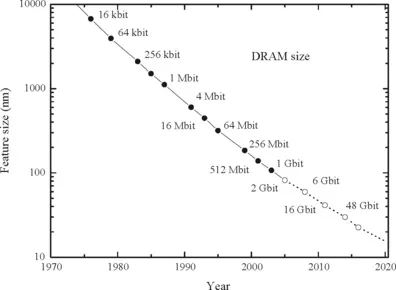
Figure 1.1 Evolution of the minimum feature size of a Si DRAM. After [1].
In the near future, and due to the growing demands of calculus from industries like communications, information, military, space, etc. microelectronics will be replaced by nanoelectronics since the feature size of electronic devices will be reduced to about 10 nm. Although there has been an impressive advance at the device and technology level during the last decade, the progress in the development of new system architectures dealing with billions of transistors is scarce. In this sense, new architectures for parallel data processing are under current development.
The evolution towards nanoelectronics has been possible because of advances in the deposition of very thin films to form heterostructures in which electrons could be confined to a 2D mesoscopic system. Standard evaporation and sputtering techniques did not produce heter...
Table of contents
- Cover image
- Title page
- Table of Contents
- Elsevier Internet Homepage
- Copyright
- Preface
- About the Authors
- Acknowledgements
- Structure of the Book
- Chapter 1: Mesoscopic Physics and Nanotechnologies
- Chapter 2: Survey of Solid State Physics
- Chapter 3: Review of Semiconductor Physics
- Chapter 4: The Physics of Low-Dimensional Semiconductors
- Chapter 5: Semiconductor Quantum Nanostructures and Superlattices
- Chapter 6: Electric Field Transport in Nanostructures
- Chapter 7: Transport in Magnetic Fields and the Quantum Hall Effect
- Chapter 8: Optical and Electro-optical Processes in Quantum Heterostructures
- Chapter 9: Electronic Devices Based on Nanostructures
- Chapter 10: Optoelectronic Devices Based on Nanostructures
- Index
Frequently asked questions
Yes, you can cancel anytime from the Subscription tab in your account settings on the Perlego website. Your subscription will stay active until the end of your current billing period. Learn how to cancel your subscription
No, books cannot be downloaded as external files, such as PDFs, for use outside of Perlego. However, you can download books within the Perlego app for offline reading on mobile or tablet. Learn how to download books offline
Perlego offers two plans: Essential and Complete
- Essential is ideal for learners and professionals who enjoy exploring a wide range of subjects. Access the Essential Library with 800,000+ trusted titles and best-sellers across business, personal growth, and the humanities. Includes unlimited reading time and Standard Read Aloud voice.
- Complete: Perfect for advanced learners and researchers needing full, unrestricted access. Unlock 1.5M+ books across hundreds of subjects, including academic and specialized titles. The Complete Plan also includes advanced features like Premium Read Aloud and Research Assistant.
We are an online textbook subscription service, where you can get access to an entire online library for less than the price of a single book per month. With over 1.5 million books across 990+ topics, we’ve got you covered! Learn about our mission
Look out for the read-aloud symbol on your next book to see if you can listen to it. The read-aloud tool reads text aloud for you, highlighting the text as it is being read. You can pause it, speed it up and slow it down. Learn more about Read Aloud
Yes! You can use the Perlego app on both iOS and Android devices to read anytime, anywhere — even offline. Perfect for commutes or when you’re on the go.
Please note we cannot support devices running on iOS 13 and Android 7 or earlier. Learn more about using the app
Please note we cannot support devices running on iOS 13 and Android 7 or earlier. Learn more about using the app
Yes, you can access Nanotechnology for Microelectronics and Optoelectronics by Raúl José Martín-Palma,José Martínez-Duart,Fernando Agullo-Rueda in PDF and/or ePUB format, as well as other popular books in Technology & Engineering & Electrical Engineering & Telecommunications. We have over 1.5 million books available in our catalogue for you to explore.