eBook - ePub
Semiconductor Safety Handbook
Safety and Health in the Semiconductor Industry
- 634 pages
- English
- ePUB (mobile friendly)
- Available on iOS & Android
eBook - ePub
About this book
Interwoven within our semiconductor technology development had been the development of technologies aimed at identifying, evaluating and mitigating the environmental, health and safety (EH&S) risks and exposures associated with the manufacturing and packaging of integrated circuits. Driving and advancing these technologies have been international efforts by SEMI's Safety Division, the Semiconductor Safety Association (SSA), and the Semiconductor Industry Association (SIA). The purpose of the Semiconductor Safety Handbook is to provide a current, single source reference for many of the primary semiconductor EH&S technologies and disciplines. To this end, the contributors have assembled a comprehensive text written by some of the leading experts in EH&S in the semiconductor industry. This text had taken three years to complete and has involved tremendous effort and commitment by the authors.They have attempted to construct a reference manual that is comprehensive in its coverage of the technical aspects of each individual subject, while at the same time addressing practical applications of each topic. The scope of this text, from its inception, was intended to address significantly more than what would typically be classified under the definition of ""safety."" However, all of the chapters have a direct application to the protection and preservation of semiconductor employees, the surrounding communities and the environment.This book is a hands-on reference to environmental, health and safety issues critical to the semiconductor industry. It was also the author's intent to produce a text that provides a practical user's guide for semiconductor environmental, health and safety practitioners as well as those individuals responsible for operation, maintenance and production in wafer fabrication facilities.
Trusted by 375,005 students
Access to over 1.5 million titles for a fair monthly price.
Study more efficiently using our study tools.
Information
1 Injury and Illness of Semiconductor Workers: Experience and Epidemiologic Studies
1.0 INTRODUCTION
The U.S. semiconductor industry workplace presents an interesting departure from the classic view of the American working environment. As the very essence of what has become known as “High Technology” or the “High Tech” industry, the semiconductor industry is characterized by rapid changes, based on intense competition to place increasingly smaller microcircuits on increasingly smaller substrate surfaces, with no loss in final product “yield.” Layered on top of competitive production change is the necessity to perform the crucial elements of manufacturing in isolated, ultra-clean wafer fabrication units. Workers themselves are further isolated from the product being produced by wearing special “gowns,” hair covers and facial masks. They are protected from harmful exposures to toxic chemicals and physical agents in ways that no large, manufacturing work force has ever been protected previously. Only the aerospace and nuclear weapons industries provide similar worker exposure controls. Yet, in all three of these industries, worker exposure controls were designed primarily to maintain product purity in a working environment free of harmful contamination. Practically speaking, concerns for product purity have resulted also in worker protection.
The wearing of personal protective clothing in semiconductor wafer fabrication rooms has been coupled with sophisticated systems of ventilation and chemical/gas air monitoring and detection. Alarms can be set at parts per million (ppm), or even parts per billion (ppb), to ensure that semiconductor employees are protected from harmful exposures resulting from releases of monitored chemical and gaseous substances. From this perspective, it must be understood that such controls on monitoring workplace air are absolutely essential in the wafer “fab.” Extremely toxic gases, such as arsine, phosphine and diborane have been in use in wafer fabrication since the beginning of the industry. The history of the industry is replete with wafer fab evacuations based on real or suspected leaks of gases or of solvents. Such evacuation episodes have become much less frequent in today’s wafer fabs largely because of the lessons learned in design of ventilation systems, toxic gas/chemical handling and increasingly sophisticated air monitoring systems with continuous air sampling.
From the standpoint of traditional workplace injury and illness statistics, the U.S. semiconductor industry has provided a model for worker safety and health protection. The frequency of work-related accidents and exposures resulting in injuries and illnesses has been among the lowest in the U.S. Figure 1 provides a graphic illustration of this experience compared with the private sector, all U.S. manufacturing, and durable goods manufacturing. However, the industry has not been free of work injuries and illnesses, even though the rate of occurrence of such conditions has been low. Nor has the industry been free of concern that more subtle health effects may be present.[1]
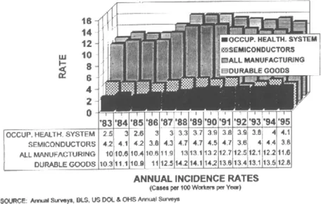
Figure 1 Comparative annual incidence rates for Occupational Health System, U.S. semiconductor industry, durable goods, and all manufacturing (1983–95).
In this chapter, we attempt to address both aspects of the U.S. semiconductor injury and illness experience. The chapter will skim over the past decade characterized by very low incidence rates of work injuries and illnesses among semiconductor workers to focus, instead, on stratification of work injuries and illnesses experienced by this work force during 1993 (provided by the U.S. Bureau of Labor Statistics and the Occupational Health System of the Semiconductor Industry Association).[2] Because of a major concern for the reproductive health of workers which surfaced in this industry during the middle 1980’s, a review of three, independent epidemiologic investigations is presented and the results discussed.
Finally, it must be emphasized that the U.S. semiconductor industry has represented a unique modeling opportunity for public health research. Although major companies within the industry have always been highly competitive, these same companies have formed several organizations designed to facilitate information and data exchange of a noncompetitive nature which have relevance to the safety and health of the semiconductor work force. These organizations include SEMATECH, the Semiconductor Safety Association (SSA), and the Environmental Safety and Health Committee of the Semiconductor Industry Association (SIA). The geographic “compactness” of the industry in the “Silicon Valley” of Northern California in the 1980’s made possible the development of the Occupational Health System (OHS), which will be discussed later. Without the ability to maintain a close, ongoing relationship with key members of the industry’s safety and health community (often involving ad hoc meetings on short notice) a work injury and illness surveillance system such the OHS might not have been possible.
2.0 REVIEW AND DISCUSSION OF SEMICONDUCTOR INDUSTRY WORK INJURIES AND ILLNESSES
During the past several decades the primary indicator of the safety and health experience of the American work force has been the incidence of work-related injuries and illnesses as published annually by the U.S. Bureau of Labor Statistics (BLS).[3] These incidence rates (calculated as the average number of new injury or illness cases per 100 full-time equivalent employees per year) have provided a standardized annualized statistic for comparing the overall work injury and illness experience of workers in various industry sectors.
Prior to 1972 (the initial BLS survey year), the only significant sources of data concerning semiconductor worker safety and health were individual states ‘workers’ compensation records. Because of the dearth of data concerning worker health prior to 1972, the growth of the industry during the 1970’s and the many manufacturing process changes which have become a signature of the industry, historical data concerning injuries and illnesses among semiconductor workers prior to 1972 can be considered fairly irrelevant.
Hence, the safety and health experience of the U.S. semiconductor industry work force has been closely tied to the annual incidence of work injuries and illnesses as calculated by the BLS rate for this industry. Figure 1 compares annual incidence rates for various industry sectors with the rates for the semiconductor industry during the period 1983–1995.
Beginning in 1982, the primary trade association of the U.S. semiconductor industry (Semiconductor Industry Association—SIA) has sponsored the development and maintenance of the Occupational Health System (OHS). This system provides detailed data analyses of pertinent work injury and illness case variables on an annual basis for the semiconductor industry. Approximately one-quarter to one-third of the U.S. semiconductor industry participates in the OHS program on a year-to-year basis. Prior to 1982, the only significant data concerning the safety and health experience of the nation’s semiconductor work force were those published annually in the BLS surveys, as discussed above.
Other indicators of the safety and health status of semiconductor workers have been reports of surveys (Health Hazard Evaluations) performed by the National Institute for Occupational Safety and Health (NIOSH), a sprinkling of papers published in the open scientific literature and proceedings of symposia associated with environmental and worker safety and health issues.[4][5] In addition, an annual meeting of semiconductor safety, health and environmental professionals sponsored by the Semiconductor Safety Association (SSA) has provided timely presentations concerning worker safety and health issues.
Finally, as stated above, several epidemiologic studies have been performed during the past decade which focus on reproductive health consequences of employment in the semiconductor industry.
These sources of data and information c...
Table of contents
- Cover image
- Title page
- Table of Contents
- About the Editor
- Copyright
- SEMICONDUCTOR SAFETY SERIES
- Preface
- Contributors
- NOTICE
- Chapter 1: Injury and Illness of Semiconductor Workers: Experience and Epidemiologic Studies
- Chapter 2: Environmental Compliance in the Semiconductor Industry: Detection, Correction and Prevention
- Chapter 3: APPENDIX A: EPA POLICY ON ENVIRONMENTAL AUDITING
- Chapter 4: APPENDIX B: Environmental Compliance Audit Checklist
- Chapter 5: APPENDIX C
- Chapter 6: Chemical Hazards in Semiconductor Operations
- Chapter 7: Industrial Hygiene
- Chapter 8: Electrical Hazards
- Chapter 9: Radiation Safety
- Chapter 10: Recognition, Evaluation and Control of Some Plasma Processing Hazards
- Chapter 11: Fire Protection Technology for Semiconductor Operations
- Chapter 12: Building and Fire Codes Impacting the Semiconductor Industry
- Chapter 13: Gases and Gas Equipment
- Chapter 14: Toxic Gas Monitoring
- Index
Frequently asked questions
Yes, you can cancel anytime from the Subscription tab in your account settings on the Perlego website. Your subscription will stay active until the end of your current billing period. Learn how to cancel your subscription
No, books cannot be downloaded as external files, such as PDFs, for use outside of Perlego. However, you can download books within the Perlego app for offline reading on mobile or tablet. Learn how to download books offline
Perlego offers two plans: Essential and Complete
- Essential is ideal for learners and professionals who enjoy exploring a wide range of subjects. Access the Essential Library with 800,000+ trusted titles and best-sellers across business, personal growth, and the humanities. Includes unlimited reading time and Standard Read Aloud voice.
- Complete: Perfect for advanced learners and researchers needing full, unrestricted access. Unlock 1.5M+ books across hundreds of subjects, including academic and specialized titles. The Complete Plan also includes advanced features like Premium Read Aloud and Research Assistant.
We are an online textbook subscription service, where you can get access to an entire online library for less than the price of a single book per month. With over 1.5 million books across 990+ topics, we’ve got you covered! Learn about our mission
Look out for the read-aloud symbol on your next book to see if you can listen to it. The read-aloud tool reads text aloud for you, highlighting the text as it is being read. You can pause it, speed it up and slow it down. Learn more about Read Aloud
Yes! You can use the Perlego app on both iOS and Android devices to read anytime, anywhere — even offline. Perfect for commutes or when you’re on the go.
Please note we cannot support devices running on iOS 13 and Android 7 or earlier. Learn more about using the app
Please note we cannot support devices running on iOS 13 and Android 7 or earlier. Learn more about using the app
Yes, you can access Semiconductor Safety Handbook by Richard A. Bolmen in PDF and/or ePUB format, as well as other popular books in Technology & Engineering & Quantum Theory. We have over 1.5 million books available in our catalogue for you to explore.