![]()
CHAPTER 1
Introduction and Fundamental Principles of Ambipolar Materials
Yi Ren a , Su-Ting Han*b and Ye Zhou*a
a Institute for Advanced Study, Shenzhen University, Shenzhen, 518060, PR China,
b Shenzhen Key Laboratory of Flexible Memory Materials and Devices, Institute of Microscale Optoelectronics, Shenzhen University, Shenzhen, 518060, PR China,
*E-mail:
[email protected] ,
[email protected] This book focuses on ambipolar materials and related devices. An introductory description on the fundamental properties and theories of ambipolar materials and devices is first presented. Then, the synthesis and properties of various state-of-the-art ambipolar materials, the operation principles and electrical performance of their devices, as well as several ambipolar device architectures are discussed. Various applications based on ambipolar devices are also presented. Lastly, we point out the remaining challenges, comprising material design and device fabrication, that need to be confronted in achieving ambipolar charge transport, and propose several possible strategies.
1.1 Introduction
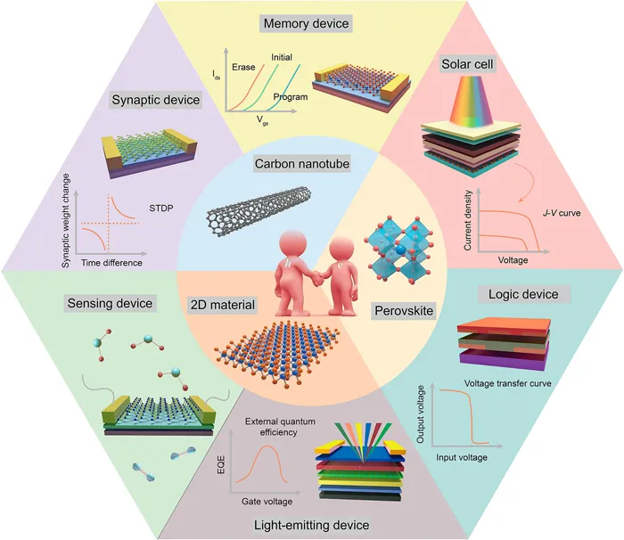
In the modern era, extensive research in the emerging internet of things and artificial intelligence has provided significant impetus for technological advances in information networks. In order to achieve the complicated functions for the internal circuits required, various stable materials and primary circuit elements are essential as basic functional modules. Therefore, exploration of novel multifunctional materials and devices, as well as miniaturization and high density integration of functional materials and devices, has been the goal of scientific researchers. When incorporating inherent materials into electronic devices, the charge transport properties can be evaluated. In terms of their electrical properties and the principal conductive carriers in devices, materials or devices can be classified into two types: unipolar and ambipolar. Unipolar devices include p-type and n-type devices, where the predominant conductive charges are holes and electrons, respectively. This type of device exhibits relatively unitary electrical characteristics and hence their application ranges have certain limitations. Ambipolar materials and devices, however, can realize comparable simultaneous transfer of electrons and holes, and thereby display p-type and n-type characteristics within a single device, which makes them useful in many different fields. 1,2 In the last few years, diverse ambipolar materials, such as organic materials, 3 carbon nanotubes, 4 two-dimensional (2D) 5 and perovskite materials, 6 and various device architectures, for instance, bilayer 7 and blended structures, 8 have been produced to achieve ambipolar carrier conduction and further applications, comprising solar cells, 9 logic devices, 10 neuromorphic devices, 11 light-emitting transistors (LETs), 12 gas sensors 13 and ambipolar flash memory 14 (see Figure 1.1). Ambipolar materials and devices have been investigated and applied in printed electronics owing to the fact that their intrinsic properties, with concurrent transport of holes and electrons, can greatly enhance the electrical performance of devices, reduce the fabrication complexity, as well as generate novel electrical and optoelectronic phenomena.
Figure 1.1 A schematic illustration of various ambipolar materials and devices.
This book focuses on ambipolar materials and devices. The outline of this book is described below. An introductory description on the fundamental properties and theories of ambipolar materials and devices is presented first. Then, the synthesis and properties of various state-of-the-art ambipolar materials (e.g., organic polymers and 2D materials), the operation principles and electrical performance of their devices, as well as several ambipolar device architectures are reviewed and analyzed in detail. Within these described material and device systems, despite inherent challenges, the fundamentals and physics of the ambipolar materials and devices have been well understood and thereby numerous functional applications have begun to emerge. Therefore, many applications based on ambipolar devices, for instance, gas sensors and LETs, are also discussed. Lastly, we point out the remaining challenges for material design and device fabrication that are faced in achieving ambipolar charge transport, and propose several possible solution strategies.
1.2 Fundamentals of Ambipolar Materials
1.2.1 Ambipolar Organic Materials
Organic materials, including small molecules and polymers, can be engineered and modified to acquire specific energy levels and charge transport characteristics. 15 Besides, organic materials are also readily scaled up and can be separated with relatively high purity. Thus, organic materials, such as conjugated polymers containing isoindigos and diketopyrrolopyrroles (DPPs), can be utilized to realize good ambipolar behaviors, with large charge mobility and on/off ratio, when exploited as semiconductors in thin-film transistors. 16,17 In order to obtain ambipolar carrier conduction, both types of charge carriers should be injected effectively from the metal electrodes to the organic semiconducting materials. 1 This means that the highest occupied molecular orbital (HOMO) and lowest unoccupied molecular orbital (LUMO) energy levels of the organic semiconductors are supposed to be aligned with the work function of the metal electrodes for efficient hole and electron injection, respectively. 2 However, most organic materials still present unipolar phenomena (mostly hole-dominated p-type behavior) because they possess relatively large energy gaps (2–3 eV) and hence at least one type of charge carrier cannot be injected efficiently for given specific metal electrodes. 18 In this regard, organic materials with a considerably smaller energy gap of less than 2 eV are favorable for realizing a decreased injection barrier for holes and electrons and, thereby, ambipolar charge transport. In addition, a narrow band gap with a lowered LUMO level is also capable of improving the air stability of ambipolar materials significantly, as a result of the reduced captured charges by O2 or H2O in ambient air. 19 Furthermore, the morphology of organic thin films (with various molecular packing modes and crystallinities) can also impact the ambipolar performance, for instance, the mobilities of charge carriers. 20 For the sake of forming a superior morphology for the organic active layer, the appropriate design of molecular structures, 21 optimized fabrication methods and preparation conditions, 22 as well as substrate modification, 23 are all essential.
1.2.2 Carbon Nanotubes
Semiconducting single-walled carbon nanotubes (SWNTs) possess remarkable mobilities of charges, and energy gaps of approximately 0.7–1 eV dominated by their intrinsic size. 24 Additionally, they are intrinsic semiconductors with a direct band gap property, which makes it possible for them to transport both two types of charge carriers. The SWNT networks can be manufactured via utilizing various approaches, such as chemical vapor deposition and solution deposition. 25 For the latter, different deposition approaches give rise to plentiful and various carbon nanotubes. Thus selective separation of the metallic nanotubes and realization of SWNTs with single chirality and regulated length are both necessary to acquire pure and well-dispersed nanotube inks. So far, many effective post-synthetic separation methods have been proposed to sort and purify the nanotubes, for instance, polymer sorting, 26 gel chromatography, 27 density gradient ultracentrifugation, 28 DNA-based separation 29 and electrophoresis. 30 Among them, selective solubilization by polymer sorting is more efficient and the backbones, as well as the side chains, of organic polymeric materials can select and purify the nanotubes based on the non-covalent interactions between them. 31,32 However, intrinsic ambipolar nanotubes generally exhibit hole accumulation behavior under ambient conditions by reason of the existence of abundant H2O and O2, the interface capture of electrons induced by hydroxyl groups, as well as the formation of a relatively large energy barrier for electron injection. Thus, several effective strategies, such as usage of high k-blocking dielectric, 33 n-type doping, 34 suitable electrodes with relatively little contact resistance, 35 as well as ionic gating, 36 have been put forward to achieve ambipolar carrier conduction. In addition, a dual-gate configuration, composed of original and control gates, is also effective and can regulate and manage the longitudinal electrical field and hence the internal electrons and holes, which finally results in adjustable charge polarity. 37
1.2.3 Ambipolar 2D Materials
Two-dimensional layered materials, for instance, transition metal dichalcogenides (TMDs) and graphene, have been extensively studied and exploited as significant functional layers within various electronic and optoelectronic devices as a result of their superior optoelectronic and mechanical properties. 9 Besides, because the effective mass of electrons can be ignored in a Fermi surface, relatively large mobilities of both types of charge car...