- 336 pages
- English
- ePUB (mobile friendly)
- Available on iOS & Android
eBook - ePub
Integrated Circuit Fabrication
About this book
This book covers theoretical and practical aspects of all major steps in the fabrication sequence. This book can be used conveniently in a semester length course on integrated circuit fabrication. This text can also serve as a reference for practicing engineer and scientist in the semiconductor industry. IC Fabrication are ever demanding of technology in rapidly growing industry growth opportunities are numerous. A recent survey shows that integrated circuit currently outnumber humans in UK, USA, India and China. The spectacular advances in the development and application of integrated circuit technology have led to the emergence of microelectronic process engineering as an independent discipline. Integrated circuit fabrication text books typically divide the fabrication sequence into a number of unit processes that are repeated to form the integrated circuit. The effect is to give the book an analysis flavor: a number of loosely related topics each with its own background material.
Note: T& F does not sell or distribute the Hardback in India, Pakistan, Nepal, Bhutan, Bangladesh and Sri Lanka.
Trusted by 375,005 students
Access to over 1.5 million titles for a fair monthly price.
Study more efficiently using our study tools.
Information
1
Introduction to Silicon Wafer Processing
1.1 INTRODUCTION
Designing a complex electronic machine of compact size like a laptop or mobile, it is always desired and necessary to increase the number of components involved in order to make technical advanced. The logic operation parts of the machines are conducted through integrated circuits made of semiconductor material. The monolithic integrated circuit placed the previously separated diodes, transistors, resistors, capacitors and all the connecting wiring onto a single crystal (or ‘chip’). The monolithic integrated circuit was fated to be invented as two inventors who were unaware of each others activities, invented almost identical integrated circuits or ICs at nearly the same time.
Jack Kilby, an engineer from Texas Instruments in 1958 with a background in ceramic-based silk screen circuit boards and transistor-based hearing aids had similar idea of making a whole circuit on a single chip as of research engineer Robert Noyce who had co-founded the Fairchild Semiconductor Corporation in 1957.
What we didn’t realize then was the integrated circuit would reduce the cost of electronic functions by a factor of a million to one, nothing had ever done that for anything before” - Jack Kilby
In 1961 the first commercially available integrated circuits came from the Fairchild Semiconductor Corporation.
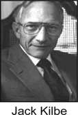
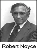
Fig. 1.1 Photo image of (a) Jack Kilbe (b) Robert Noyce
Jack Kilby holds patents on more than sixty inventions and is also well known as the inventor of the portable calculator (1967), awarded the National Medal of Science in 1970. Robert Noyce, with sixteen patents to his name, founded Intel, the company responsible for the invention of the microprocessor, in 1968. The invention of the integrated circuit by both men stands historically as one of the most important innovations of mankind as almost all modern products use chip technology. Kilby used Germanium and Noyce used silicon for the semiconductor material.
All computers then started to be made using chips instead of assembling the individual transistors and their accompanying parts. Texas Instruments first used the chips in Air Force computers and the Minuteman Missile in 1962. They later used the chips to produce the first electronic portable calculators. The first IC had only one transistor, three resistors, and one capacitor having a size of an adult’s pinkie finger. Today an IC smaller than a penny can hold more than 1 billion transistors.
The advantages of integrated circuits are as follows
- Small in size due to the reduced device dimension
- Low weight due to very small size
- Low power requirement due to lower dimension and lower threshold power requirement
- Low cost due to large-scale production and cheap material
- High reliability due to the absence of a solder joint
- Provide facilitation to integrate large number of devices and components.
- Improves the device performance even at high-frequency region
The disadvantages of integrated circuits are as follows
- IC resistors have a limited range
- Due to bulky size generally inductors (L) cannot be formed using IC
- Transformers cannot be formed using IC.
1.2 VLSI GENERATIONS
Historically, the first semiconductor IC chips held one transistor with three resistors and one capacitor. Advancement of technology enabled us to add more and more number of transistors.
The first to arrive was Small-Scale Integration (SSI), then improvements in technique led to devices with millions to billions of logic gates-Very Large- Scale Integration (VLSI).
Present day’s microprocessors have millions of logic gates and transistors. Intel co-founder, Gordon E. Moore, in 1965 published a paper on the future projection of IC technology.
Moore’s Law is responsible for “smaller, compact, cheaper and more efficient IC”. Gordon Moore’s empirical relationship is cited in a number of forms, but its essential thesis is that the numbers of transistors that can be manufactured on a single die will double every 18 months.
Wickes (1969) in his paper categorizes between SSI, MSI and LSI by the number of logic gates implemented on single chip where single equivalent logic gate is taken as the fundamental building block. On this basis a SSI circuit is one which has 1~10 equivalent logic gates, an MSI circuit is one which has 10~100 logic gates and LSI circuit is one which has more than 100 logic gates. (e.g., random access bipolar memory modules have approximately 500 equivalent gates and other advanced modules are expected to have four times the number.) After the success of LSI, the era of Very Large Scale Integration (VLSI), Extra Large Scale Integration (ELSI), Ultra Large Scale Integration (ULSI), etc has begun with having the ability to perform a very complex logic function, or a large number of simple logic functions in very short time.
The first generation integrated circuits contained only a few transistors called “Small-Scale Integration” (SSI), they used circuits containing transistors numbering in the tens.
SSI circuits were used in early Aerospace project and Missile projects. The two major program of that time, Minuteman missile and Apollo program needed lightweight digital computers for their inertial guidance systems. The Apollo guidance computer motivated the integrated-circuit technology, while the Minuteman missile forced it into mass-production which led SSI to become commercial. These programs acquired almost all of the available integrated circuits from 1960 through 1963, and almost alone provided the demand that funded the production improvements to get the production costs from $1000/circuit (in 1960 dollars) to merely $25/circuit (in 1963 dollars). After the successful implementation in defense industry they began to appear in consumer products a typical application being FM inter-carrier sound processing in television receivers.
In the late 1960s, the next step in the development of integrated circuit was taken with introduction of devices that contained hundreds of transistors on each chip, called Medium-Scale Integration” (MSI).
They were more attractive and fast processing then SSI because, they allowed more complex systems to be produced using smaller circuit boards, less assembly work (because of fewer separate components), and a number of other advantages but they cost little more to produce than SSI devices.
First and second generation microprocessor, computer memories, calculator chips led further development of IC for mass commercial production so Large Scale Integration (LSI) circuits come into picture in the early 1970s that contain tens of thousand transistors on each chip and finally in 1974 to Very Large Scale Integration (VLSI) circuits containing hundreds of thousands transistors on each chip in early 1980s and continues to millions transistors. This led to increase production of chips utilizing then in different new products also the shrinking of chip size and reduction of chip cost.
Figure 1.2 gives the way of dividing discussion on LSI technology on a number of dimensions.
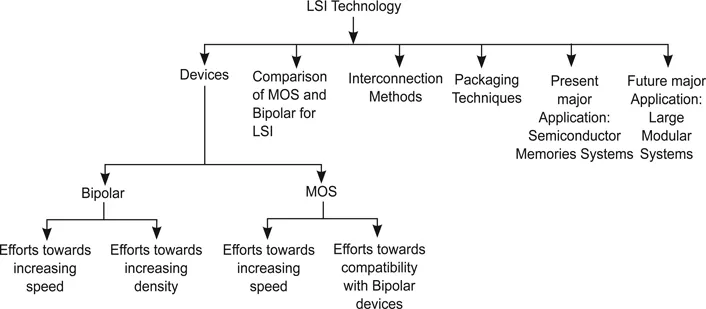
Fig. 1.2 LSI Technology
| Scale of Integration | No of Transistor | Function | Time |
|---|---|---|---|
| SSI | Fewer than 10 | Input and output gates are connected directly to package | 1963 |
| MSI | 10 to 99 | Performs digital function like decoders, adders, registers | 1970 |
| LSI | 100 to 9999 | Includes digital systems such as processors, memory chips and programmable modules | 1975 |
| VLSI/ULSI | 10000 to 99999 | Include large memory array and complex microcomputer chips | 1980 |
In recent years the rate of growth has showed difficulties in defining, designing and processing complicated chips were about 100 million devices /chip available before 2000 and 1 billion in 2011. The devices which are used in today’s integrated circuits, primarily CMOS, Bi-CMOS, GaAs and FinFET, in 1980 at the beginning of VLSI era the minimum feature size was 2μm which shrink to 0.1 μm in 2000 and to 0.022μm in 2011. Device miniaturization results in reduced unit cost per function and in improved performance. The device speed has improved by four orders of magnitude since 1960. Higher speed leads to expanded IC functional throughput rates. Digital ICs are able to perform data processing, numerical computation and signal conditioning at 10 and higher gigabit per second rates. Another benefit is the reduction of power consume as the device become smaller so, consume less power and reduces the energy used for each switching operation.
1.3 CLEAN ROOM
In 1965 the chip manufacturing factories were filthy by toda...
Table of contents
- Cover
- Half Title
- Title Page
- Copyright Page
- Dedication Page
- Brief Contents
- Detail Contents
- Preface
- 1. Introduction to Silicon Wafer Processing
- 2. Epitaxy
- 3. Oxidation
- 4. Lithography
- 5. Etching
- 6. Diffusion
- 7. Ion Implantation
- 8. Film Deposition: Dielectric, Polysilicon and Metallization
- 9. Packaging
- 10. VLSI Process Integration
- Appendix
- Index
Frequently asked questions
Yes, you can cancel anytime from the Subscription tab in your account settings on the Perlego website. Your subscription will stay active until the end of your current billing period. Learn how to cancel your subscription
No, books cannot be downloaded as external files, such as PDFs, for use outside of Perlego. However, you can download books within the Perlego app for offline reading on mobile or tablet. Learn how to download books offline
We are an online textbook subscription service, where you can get access to an entire online library for less than the price of a single book per month. With over 1.5 million books across 990+ topics, we’ve got you covered! Learn about our mission
Look out for the read-aloud symbol on your next book to see if you can listen to it. The read-aloud tool reads text aloud for you, highlighting the text as it is being read. You can pause it, speed it up and slow it down. Learn more about Read Aloud
Yes! You can use the Perlego app on both iOS and Android devices to read anytime, anywhere — even offline. Perfect for commutes or when you’re on the go.
Please note we cannot support devices running on iOS 13 and Android 7 or earlier. Learn more about using the app
Please note we cannot support devices running on iOS 13 and Android 7 or earlier. Learn more about using the app
Yes, you can access Integrated Circuit Fabrication by Kumar Shubham,Ankaj Gupta,Shubham Kumar in PDF and/or ePUB format, as well as other popular books in Technology & Engineering & Electrical Engineering & Telecommunications. We have over 1.5 million books available in our catalogue for you to explore.