Microelectronics and Signal Processing
eBook - ePub

Microelectronics and Signal Processing

Advanced Concepts and Applications

  1. 262 pages
  2. English
  3. ePUB (mobile friendly)
  4. Available on iOS & Android
eBook - ePub

Microelectronics and Signal Processing

Advanced Concepts and Applications

About this book

This book is about general and specific areas involved in electrical and electronics engineering which comprises broad subjects such as MEMS and Microfluidics, VLSI, Communication and Signal Processing. This book discusses the recent trends in various aspects of research areas for diverse applications like biomedical, biochemical, and power source systems. It also discusses modelling, simulating, and prototyping of the different electronic-based systems for carrying out varied applications. With this book, the readers will understand the multiplatform fundamentals guiding electrical and biomedical devices that form the current features such as automation, integration, and miniaturization of a particular device.

This book showcases a unique platform as it covers the different areas of research in this trending era as a benchmark. This book is a link between the electronics and cutting-edge technologies that are being used for numerous applications representing the physical and virtual developments of electronic devices. Therefore, this book will mostly uphold the innovation and originality involved in the development of miniaturized devices, and proposing new methods, emphasizing with different areas of electrical and electronics engineering.

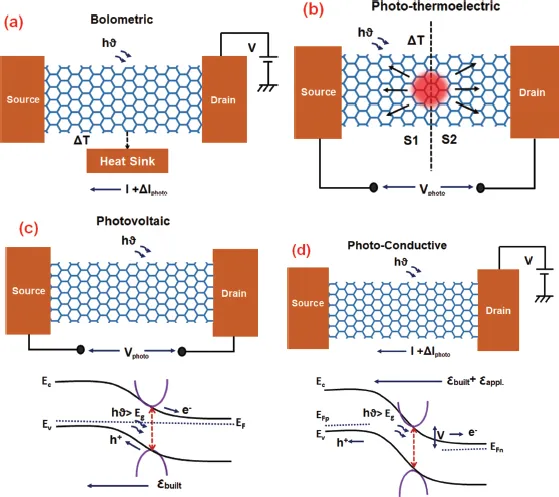
This book entitles various approaches involved in electrical, biomedical, and electronics for modern distribution of research strategies and covers the state-of-art research themes. These include signal sensing, signal simulators, 3D printing technology, power systems, data acquisition systems, instrumentation, electrochemical sensing, electromechanical measurements, and signal analysis.

The book will provide the academic perspectives of the cutting-edge R&D outputs from the faculty members and Ph.D. students, amalgamating the newer cross-dimensional areas, such as cyber-physical systems, nanoelectronics, smart-sensors, point-of-need devices, etc. The book will become a benchmark to the readers to understand the academic aspect of the contemporary work and the way forward on how this will lead to help the society-at-large.

Tools to learn more effectively

Saving Books

Saving Books

Keyword Search

Keyword Search

Annotating Text

Annotating Text

Listen to it instead

Listen to it instead

1

Van der Waals (vdW) Heterostructures Based on Transition Metal Dichalcogenides (TMD)

Current Status and Prospects in Broadband Photodetector Applications
Debapriya Som, Srijan Trivedi, Ayantika Chatterjee, and Sayan Kanungo
CONTENTS
  • 1.1 Introduction: Background
  • 1.2 General Overview of Photodetector
  • 1.3 TMD/TMD vdW Heterostructure-based Photodetector
  • 1.4 TMD/Non-TMD vdW Heterostructure
  • 1.5 Summary
  • References

1.1 Introduction: Background

The reliable detection of electromagnetic radiations over a broad spectral range is of primary interest in various fields including biomedical imaging, optical communication, environmental monitoring, food and manufacturing process monitoring, and national security and defense applications. The broadband photodetectors convert the incident electromagnetic radiations over a wide range of wavelengths into electrical signals for detection. The detection mechanism is governed by the interactions of electromagnetic radiation with photoabsorbing material and, subsequently, the choice of such material principally determines the performance of photodetectors (Konstantatos 2018; Mu, Xiang, and Liu 2017). This scenario motivated active explorations of different semiconducting materials for broadband photodetector applications. In this context, two-dimensional (2D) materials with few atomic layers thickness have shown particular promise for photodetector applications owing to their large surface area, pristine surfaces, tunable electronic properties, and mechanical flexibility. Typically, the spatial confinements of charge carriers in out-plane directions lead to high optical response and a long lifetime for photogenerated electrons and holes. Subsequently, a wide range of 2D materials is realized and eventually exploited for ultrafast and ultrasensitive detection of lights in terahertz, infrared, visible, and ultraviolet frequency ranges. In this line, transition metal dichalcogenide (TMD) has emerged as one of the potential 2D semiconductors for optoelectronic applications owing to the presence of suitable energy bandgaps (1–2 eV) that can be tuned by changing the layer thickness. Moreover, TMDs exhibit transition from an indirect to direct bandgap between their multilayers and monolayer configurations. However, like other 2D crystalline semiconductors, TMDs also suffer from low optical absorption and subsequent small photocarrier generation owing to their atomic-scale thicknesses. At the same time, the mobility of TMDs is considerably lower than Graphene (Gr), leading to a relatively slower charge transfer (Mu, Xiang, and Liu 2017; Rao et al. 2019). Therefore, significant efforts have been observed for designing novel 2D materials with superior light absorption and mobility to optimize the photoresponse.
The weak van der Waals (vdW) interaction between individual layers of 2D materials allows the realization of designer heterostructure materials by vertically stacking one or a few layers of two dissimilar 2D materials. These structures are usually referred to as vdW hetero structures having atomically sharp interfaces where emergent properties can be observed. These heterojunction materials have offered an alternative approach to enhance the overall photoresponse of the photodetector because it can exploit the combined optoelectronic properties of individual materials as well as can offer effective separation of photo-generated charge carriers due to desirable band alignment and internal electric field at the heterojunction (Cheng et al., 2014; Rao et al., 2019; Sun et al. 2017). The field of 2D vdW heterostructure-based photodetector design has considerably progressed in recent years, where TMDs remain a principal constituent of such reported vdW heterostructures. However, to the best of authors’ knowledge, to date, no exclusive review is available on TMD-based vdW heterostructure photodetectors. Subsequently, this chapter presents a comprehensive summary of TMD-based vdW heterostructure photodetectors, emphasizing the design aspects.

1.2 General Overview of Photodetector

Photodetectors are solid-state optoelectronic devices that can convert electromagnetic radiation into measurable electrical signals for the reliable detection of the former. Since the light-matter interactions in solids have manifold consequences, the different physical mechanisms can lead to the modulation in the electrical properties of solids. Therefore, based on the underlying detection mechanism, the photodetectors can be broadly classified as thermal and photon photodetectors (Mu, Xiang, and Liu 2017). In thermal photodetectors, the change in electrical properties is due to either bolometric or photothermoelectric effects that exploit the thermal effects of light absorption. The absorption of light increases the lattice temperature and thereby the phonons (quanta of lattice vibration). The subsequent change in the mobility of charge carriers modulates the photodetector current, which is termed as bolometric effects and is shown in Figure 1.1A. On the other hand, the photothermoelectric effect exploits local temperature gradient associated with light absorption to generate a voltage between the electrodes due to the spatial difference in the Seebeck coefficient (represents the temperature difference induced thermoelectric voltage in materials) as depicted in Figure 1.1B. In photon photodetectors, the photogenerated charge carrier changes the electrical properties based on either photovoltaic or photoconductive effects. The photovoltaic effect leads to a photovoltage generation in the contact electrodes of photodetector. If the photon energy of the incident radiation is higher than the bandgap of light-absorbing materials, it generates an electron-hole pair that can move under the influence of a built-in electric field that exists in the junctions and is eventually diffused to the electrodes as shown in Figure 1.1C. However, under the externally applied bias in the electrodes, the photogenerated carriers change the charge carrier density and subsequently, the terminal current. This is known as the photoconductive effect and illustrated in Figure1.1D (Mu, Xiang, and Liu 2017; Rao et al. 2019).
Each Figures represent a general 2D material with two contacts under electromagnetic illuminations. For sub-figures (a) and (d), the radiation alters the carrier mobility and carrier concentrations through bolometric and photo-conductive effect, respectively. For an applied potential difference between the contacts, such change in mobility/concentration alters the currents flowing between the contacts. Finally, for sub-figures (b) and (d), the radiation induces temperature difference and increases carrier concentrations that are spatially separated by the built-in electric field, respectively. Both of these phenomenon generate electric potential between the open circuited contacts.
FIGURE 1.1 Different physical mechanisms governing the photodetection: (A) bolometric; (B) photothermoelectric; (C) photovoltaic; and (D) photoconductive.
The performance of different photodetectors is benchmarked on the basis of a well-defined figure of merits. The key figure of merits of photodetections is as follows (Rao et al. 2019):
Responsivity (R) [unit A/W]: Defined as the ratio between the photogenerated current (Iph) and the incident power (P0) of the electromagnetic radiation
R=Iph/P0 (1.1)
External Quantum Efficiency (EQE) [unitless]: Defined as the ratio of number of photogenerated electron-hole pairs contributed to the photocurrent (Iph) to the incident photon flux (φin)
R=Iph/q ϕin (1.2)
Bandwidth (BW) [unit Hz]: Defined as the frequency of modulation for incident electromagnetic radiation that corresponds to a signal intensity typically 3 dB lower than that of continuous illumination.
Noise Equivalent Power (NEP) [unit W. (Hz)−1/2]: Defined as the minimum illumination power to achieve a unity signal-to-noise ratio at 1 Hz bandwidth.
Detectivity (D*) [unit cm. (Hz)1/2/W]: Definition of detectivity involves NEP, area (A), and BW
D=A.BW1/2/NEP (1.3)
Response Time (RT) [unit sec]: This is defined as the time required to change the signal from 10% to 90% in response to incident light intensity modulation.

1.3 TMD/TMD vdW Heterostructure-Based Photodetector

TMDs are represented as MX2, where one transition metal atom, M (Mo, W, Zr, Hf, Re) is sandwiched covalently between two same chalcogen atoms, X (S, Se, Te) and are arranged in a single atomic layer as illustrated in Figure 1.2A and 1.2B. The VIB MX2 (M = Mo, W) exhibits natural bandgaps in 2H-phase, whereas VIIB MX2 (M = Re) and IVB MX2 (M = Zr, Hf) shows natural bandgaps in 1T-phase. In general, the energy bandgaps of TMDs gradually increases with reducing layer numbers. The VIB MX2 shows direct bandgaps in their monolayer configurations. However, the IVB MX2 and VIIB MX2 remain indirect and direct bandgap semiconductors, respectively, at all layer th...

Table of contents

  1. Cover
  2. Half Title
  3. Title Page
  4. Copyright Page
  5. Dedication
  6. Contents
  7. Preface
  8. Acknowledgments
  9. About the Editor
  10. List of Contributors
  11. Chapter 1 Van der Waals (vdW) Heterostructures Based on Transition Metal Dichalcogenides (TMD): Current Status and Prospects in Broadband Photodetector Applications
  12. Chapter 2 3D Printing: A State-of-the-Art Approach in Electrochemical Sensing
  13. Chapter 3 Optimized Electrical Interface for a Vanadium Redox Flow Battery (VRFB) Storage System: Modeling, Development, and Implementation
  14. Chapter 4 A Review on Recent Advancements in Chamber-Based Microfluidic PCR Devices
  15. Chapter 5 A Classification and Evaluation of Approximate Multipliers
  16. Chapter 6 Optical MEMS Accelerometers: A Review
  17. Chapter 7 A 60-GHz SiGe HBT Receiver Front End for Biomedical Applications
  18. Chapter 8 Gate-Overlap Tunnel Field-Effect Transistors (GOTFETs) for Ultra-Low-Voltage and Ultra-Low-Power VLSI Applications
  19. Chapter 9 The Role of PMU for Frequency Stability in Hybrid Power Systems
  20. Chapter 10 A Modular Zigbee-Based IoT Platform for Reliable Health Monitoring of Industrial Machines Using ReFSA
  21. Chapter 11 A Study on Time-Frequency Analysis of Phonocardiogram Signals
  22. Chapter 12 A Study on the Performance of Solar Photovoltaic Systems in the Underwater Environment
  23. Chapter 13 A Review on Brain Tumor Segmentation Algorithms Using Recent Deep Neural Network Architectures and a Gentle Introduction to Deep Neural Network Concepts
  24. Chapter 14 LabVIEW-based Simulation Modeling of Building Load Management for Peak Load Reduction
  25. Index

Frequently asked questions

Yes, you can cancel anytime from the Subscription tab in your account settings on the Perlego website. Your subscription will stay active until the end of your current billing period. Learn how to cancel your subscription
No, books cannot be downloaded as external files, such as PDFs, for use outside of Perlego. However, you can download books within the Perlego app for offline reading on mobile or tablet. Learn how to download books offline
Perlego offers two plans: Essential and Complete
  • Essential is ideal for learners and professionals who enjoy exploring a wide range of subjects. Access the Essential Library with 800,000+ trusted titles and best-sellers across business, personal growth, and the humanities. Includes unlimited reading time and Standard Read Aloud voice.
  • Complete: Perfect for advanced learners and researchers needing full, unrestricted access. Unlock 1.4M+ books across hundreds of subjects, including academic and specialized titles. The Complete Plan also includes advanced features like Premium Read Aloud and Research Assistant.
Both plans are available with monthly, semester, or annual billing cycles.
We are an online textbook subscription service, where you can get access to an entire online library for less than the price of a single book per month. With over 1 million books across 990+ topics, we’ve got you covered! Learn about our mission
Look out for the read-aloud symbol on your next book to see if you can listen to it. The read-aloud tool reads text aloud for you, highlighting the text as it is being read. You can pause it, speed it up and slow it down. Learn more about Read Aloud
Yes! You can use the Perlego app on both iOS and Android devices to read anytime, anywhere — even offline. Perfect for commutes or when you’re on the go.
Please note we cannot support devices running on iOS 13 and Android 7 or earlier. Learn more about using the app
Yes, you can access Microelectronics and Signal Processing by Sanket Goel in PDF and/or ePUB format, as well as other popular books in Technology & Engineering & Electrical Engineering & Telecommunications. We have over one million books available in our catalogue for you to explore.