- 456 pages
- English
- ePUB (mobile friendly)
- Available on iOS & Android
eBook - ePub
GaN and Related Materials
About this book
Presents views on current developments in heat and mass transfer research related to the modern development of heat exchangers. Devotes special attention to the different modes of heat and mass transfer mechanisms in relation to the new development of heat exchangers design. Dedicates particular attention to the future needs and demands for further development in heat and mass transfer. GaN and related materials are attracting tremendous interest for their applications to high-density optical data storage, blue/green diode lasers and LEDs, high-temperature electronics for high-power microwave applications, electronics for aerospace and automobiles, and stable passivation films for semiconductors. In addition, there is great scientific interest in the nitrides, because they appear to form the first semiconductor system in which extended defects do not severely affect the optical properties of devices.
This series provides a forum for the latest research in this rapidly-changing field, offering readers a basic understanding of new developments in recent research. Series volumes feature a balance between original theoretical and experimental research in basic physics, device physics, novel materials and quantum structures, processing, and systems.
Trusted by 375,005 students
Access to over 1.5 million titles for a fair monthly price.
Study more efficiently using our study tools.
Information
CHAPTER 1 A Historical Survey of Research on Gallium Nitride
Astralux, Inc. Boulder, Colorado 80303, USA
DOI: 10.1201/9781003211082-1
Gallium nitride, GaN, was synthesized more than 50 years ago by Juza and Hahn [1] who passed ammonia over hot gallium. This method produced small needles and platelets. Their purpose was to study the crystal structure and lattice constant of GaN as part of a systematic study of many compounds. Two decades later, Grimmeiss et al. [2] used the same technique to produce small crystals of GaN for the purpose of measuring their photoluminescence spectra. Another decade later Maruska and Tietjen [3] used a chemical vapor deposition technique to make a large area layer of GaN on sapphire. All the GaN made at that time was very conducting n-type even when not deliberately doped. The donors were believed to be nitrogen vacancies. The reason for designating a N-vacancy as a donor was that a N-vacancy would form a void surrounded by four Ga atoms contributing 3 electrons. Two of these could reconstruct leaving a single electron that could be donated to the conduction band. Later this model was questioned and oxygen was proposed as the donor [4]. Oxygen with its 6 valence electrons on a N site (N has 5 valence electrons) would be a single donor. Strangely, through the 1980s no one tried a deliberate oxygen doping. However, 0-doping happened whenever air would leak accidentally into the deposition system. We had observed many times that air leaks resulted in a reddish deposit that was still very conducting but useless as a luminescent material. One day, we did a SIMS (secondary ion mass spectrometry) analysis of such a sample and found that it contained 30 at. percent of oxygen. Then it must have been gallium oxynitride. Yet, the X-ray diffraction indicated that this was still GaN, i.e., adding so much oxygen did not change the lattice constant. Perhaps this GaON deserves further study.
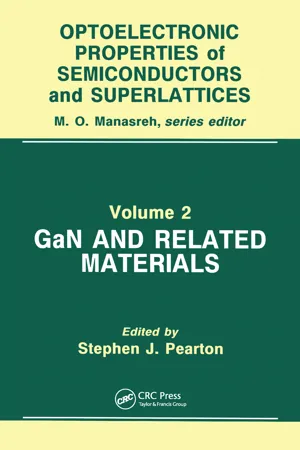
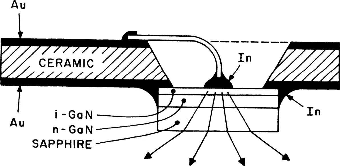
The accomplishment of Maruska and Tietjen led to a flurry of activity in many laboratories, especially when Zn-doping produced the first blue LED [5]. This was an M-i-n type of device (M: metal) (Fig. 1) that could emit either blue, green, yellow or red light depending on the Zn concentration in the light-emitting region (Fig. 2) [6]. Note that light is emitted only from the cathode. If the Zn concentration is different at the two edges of the Zn-compensated region, reversing the polarity of the bias (making the opposite interface of the i-layer the cathode) could cause a change in color, i.e., the device could switch from blue to green or to yellow. Maruska was also the first to use Mg as a luminescent center in a M-i-n diode [7].
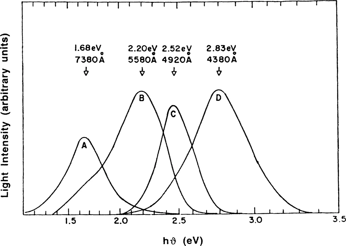
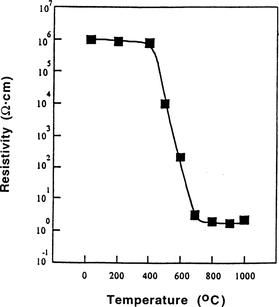
Other discoveries made with the new single crystal were: antistokes LEDs (2.8 eV photons emitted with only 1.5V applied) [8], negative electron affinity [9], surface acoustic wave generation [10], and solar-blind UV photovoltaic detectors [11]. But conducting p-type GaN was still too elusive to launch a massive effort on devices. It was the perseverance of Dr. Isamu Akasaki that eventually paid off in the pursuit of conducting p-type GaN. Actually, this was an accidental discovery: Drs. Akasaki and Amano were observing the cathodo-luminescence of GaN: Mg in an SEM (scanning electron microscope) and noticed that the brightness increased with further raster scanning. A photoluminescence study of the sample before and after the low energy electron beam irradiation (LEEBI) treatment showed that by the time the luminescence was saturated, the luminescence efficiency had increased by two orders of magnitude [12]. A Hall effect measurement showed that the layer had become p-type and conducting. As shown in Fig. 3, etching away layers of LEEBI-treated GaN : Mg revealed that the high conductivity extended only 0.3 μm deep (i.e. the penetration depth of the electron beam). This surprising phenomenon of beam-induced type conversion was explained by van Vechten et al. [13] who proposed that the shallow acceptor level of Mg was compensated by a hydrogen atom complexing with the Mg acceptor (just as H complexes with acceptors in Si [14]). The energy of the electron beam releases the hydrogen atom from this complex that then becomes a shallow acceptor about 0.16 eV above the valence band [15]. Soon thereafter, Nakamura et al. found that annealing GaN: Mg above 750°C in N2 or vacuum also converted the material to conducting p-type (Fig. 4) [16]. On the other hand, annealing in NH3 reintroduced atomic hydrogen and made GaN: Mg insulating again [16]. All this recent work led to the brightest visible LEDs available today, especially in the blue part of the spectrum [17].
A burning question in everyone’s mind has been “when shall we see a UV injection laser?”. Such a device is the much hoped for solution to the high information density compact disc vision since the areal packing density is inversely proportional to the square of the wavelength.
A 360 nm laser would allow a factor of five increase in information storage in compact discs. Although optically pumped stimulated emission in GaN has been demonstrated a long time ago [18], the electrically pumped version had remained elusive. Making a pn junction is necessary but not sufficient. The material must be of exceptionally high quality. The Nichia bright LEDs have an enormous concentration (1011 cm−2) of defects [19]. Furthermore, these LEDs have an extremely large concentration of impurities: the p-type region has one hundred times more Mg than holes, the luminescent region is an alloy of InN and GaN with undoubtedly locally varying composition. The active region is loaded with Zn that is the luminescent center; and the donor in the undoped (and the doped) regions is either N vacancies or O atoms. The evidence for the high defect concentration appears in electron microscopy studies of Lester et al. [19] and in the photoconductivity spectra of Qiu et al. [20]. The photo-conductivity spectrum reveals the presence of a high density of states in the band gap of GaN. Unlike GaAs that has an abrupt Urbach edge, GaN exhibits an extensive absorption tail (see Fig. 5). In order to obtain a low threshold injection laser with GaN, one must eliminate the absorption losses due to absorption at the lasing wavelength. The most efficient lasing should be due to the stimulation of exciton recombination. However, excitons are destroyed by local fields in heavily perturbed semiconductors. Quantum wells of InN between GaN barriers are suitable for a wide range of lasing wavelengths tunable by the width of the wells. Thin strained lattice quantum wells are desirable to overcome the lattice mismatch between InN and GaN. Doping the wells is undesirable because doping leads to level broadening and increased sub-bandgap absorption. A structure with multiple quantum wells spaced half a wavelength apart λ/2n (λ = wavelength in free space, n = refractive index of GaN at λ) has been proposed earlier [21]. Such a structure (Fig. 6) forms a surface emitting laser and provides coherence by distributed feedback rather than by resona...
Table of contents
- Cover Page
- Half-Title Page
- Title Page
- Copyright Page
- Table of Contents
- About the Series
- Introduction
- 1 A Historical Survey of Research on Gallium Nitride
- 2 Growth of Group III Nitrides from Molecular Beams
- 3 Ternary Alloys
- 4 Optical Characterisation of GaN and Related Materials
- 5 Microstructure of Epitaxial III–V Nitride Thin Films
- 6 Theoretical Studies in GaN
- 7 GaAsN Alloys and GaN/GaAs Thin-Layer Structures
- 8 The Contribution of Defects to the Electrical and Optical Properties of GaN
- 9 Growth of GaN Single Crystals Under High Nitrogen Pressure
- 10 Physical Properties of the Bulk GaN Crystals Grown by the High-Pressure, High-Temperature Method
- 11 The Role of Hydrogen in GaN and Related Compounds
- 12 Ion Implantation Doping and Isolation of III-Nitride Materials
- 13 High-Density ECR Etching of Group-III Nitrides
- 14 Contacts on III-Nitrides
- 15 III-V Nitride Based LEDs
- 16 III-V Nitride Electronic Devices
- Index
Frequently asked questions
Yes, you can cancel anytime from the Subscription tab in your account settings on the Perlego website. Your subscription will stay active until the end of your current billing period. Learn how to cancel your subscription
No, books cannot be downloaded as external files, such as PDFs, for use outside of Perlego. However, you can download books within the Perlego app for offline reading on mobile or tablet. Learn how to download books offline
Perlego offers two plans: Essential and Complete
- Essential is ideal for learners and professionals who enjoy exploring a wide range of subjects. Access the Essential Library with 800,000+ trusted titles and best-sellers across business, personal growth, and the humanities. Includes unlimited reading time and Standard Read Aloud voice.
- Complete: Perfect for advanced learners and researchers needing full, unrestricted access. Unlock 1.5M+ books across hundreds of subjects, including academic and specialized titles. The Complete Plan also includes advanced features like Premium Read Aloud and Research Assistant.
We are an online textbook subscription service, where you can get access to an entire online library for less than the price of a single book per month. With over 1.5 million books across 990+ topics, we’ve got you covered! Learn about our mission
Look out for the read-aloud symbol on your next book to see if you can listen to it. The read-aloud tool reads text aloud for you, highlighting the text as it is being read. You can pause it, speed it up and slow it down. Learn more about Read Aloud
Yes! You can use the Perlego app on both iOS and Android devices to read anytime, anywhere — even offline. Perfect for commutes or when you’re on the go.
Please note we cannot support devices running on iOS 13 and Android 7 or earlier. Learn more about using the app
Please note we cannot support devices running on iOS 13 and Android 7 or earlier. Learn more about using the app
Yes, you can access GaN and Related Materials by Stephen J. Pearton in PDF and/or ePUB format, as well as other popular books in Technology & Engineering & Thermodynamics. We have over 1.5 million books available in our catalogue for you to explore.