Atomic force microscopy (AFM) can be used to analyze and measure the physical properties of all kinds of materials at nanoscale in the atmosphere, liquid phase, and ultra-high vacuum environment. It has become an important tool for nanoscience research. In this book, the basic principles of functional AFM techniques and their applications in energy materials—such as lithium-ion batteries, solar cells, and other energy-related materials—are addressed.
FEATURES
First book to focus on application of AFM for energy research
Details the use of advanced AFM and addresses many types of functional AFM tools
Enables readers to operate an AFM instrument successfully and to understand the data obtained
Covers new achievements in AFM instruments, including electrochemical strain microscopy, and how AFM is being combined with other new methods such as infrared (IR) spectroscopy
With its substantial content and logical structure, Atomic Force Microscopy for Energy Research is a valuable reference for researchers in materials science, chemistry, and physics who are working with AFM or planning to use it in their own fields of research, especially energy research.
Trusted by 375,005 students
Access to over 1.5 million titles for a fair monthly price.
Scanning probe microscopy (SPM) is able to measure the surface morphology and the physical/chemical functionalities of materials with high spatial resolution, on the basis of the interaction between sample surface and probe. In SPM family, scanning tunneling microscopy (STM) and atomic force microscopy (AFM) were invented successively in 1980s.1,2 For STM, the topographic imaging depends on the quantum tunneling effect. It obtains the topography on atomic scale by collecting the tunneling current in a separation between the conductive tip with a sharp apex and the measured surface. STM is only used to measure the topography for conductor and semiconductor materials. Fortunately, AFM overcomes this restriction and is competent for imaging morphology of insulator materials, with nanometric resolution in lateral x/y direction and vertical (z) resolution of beyond 0.1 nm in some cases.
As one of the near-field techniques, AFM presents many strengths: (1) ultrahigh spatial resolution of reaching the sub-nanometric scale; (2) better force control in the range of nano-to-micro newton between AFM tip and the sample; and (3) easy specimen preparation and flexible imaging environments such as vacuum, air, and liquid. In addition, other than the surface morphology, AFM allows synchronous quantified characterizations for chemical, mechanical, electrical, and magnetic properties of functional materials. An AFM probe could be regarded as a nano “operator” to manipulate chemical or physical properties such as chemical etching, electric polarization, and atom/molecule migration.
In this chapter, the fundamental working principles and classic imaging modes of AFM will be first reviewed, followed by the discussion of force and quantitative nanoscale mechanical property imaging. Finally, recent developments in high-resolution imaging, AFM test in different environments (air, liquid, and ultrahigh vacuum), and AFM for electrical conductivity measurement will be demonstrated.
1.1 Working Principles of AFM
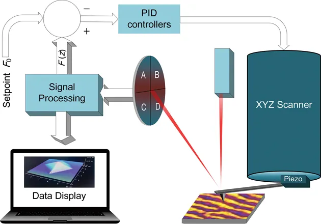
Different from the “seeing” method of the optical and electron microscopy techniques, a nanoscale probe of AFM is used to “touch” and visualize the surface morphology. An AFM system is primarily comprised of the tip-sample motion unit, the feedback system, as well as the data processing and display system, where the first two parts constitute the mainframe of AFM. An AFM probe with a micro-cantilever of about 100–500 μm in length and less than 60 μm in width is used to detect the surface topography of the sample, where one end of the cantilever probe is fixed, while the other end has a sharp tip. In the tip-sample motion unit, a piezo scanner controls the scan motion of the probe or sample with a spatial (x, y, z) accuracy in sub-nanometer level. Supposing that the scanner controls the motion of probe and the sample is immobile, a basic AFM framework is roughly sketched in Figure 1.1. Sub-nanoscale (x, y, z) positioning is driven by a piezoelectric ceramic component assembled into the scanner under high-voltage simulation.
FIGURE1.1 A schematic diagram of an AFM system.
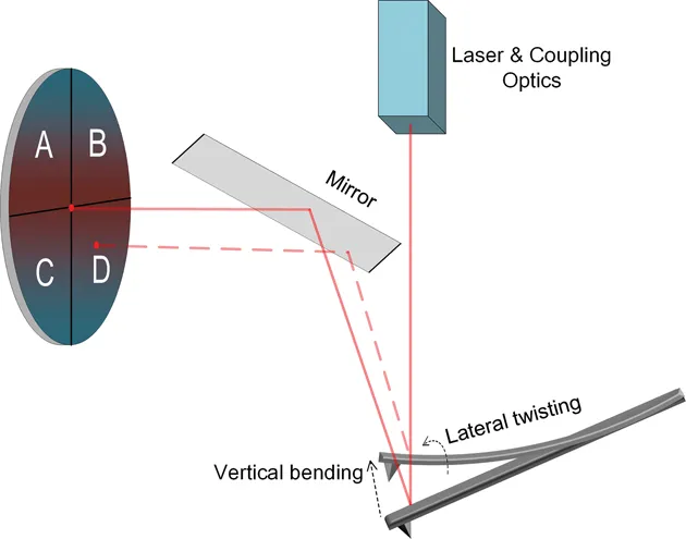
A laser beam is emitted from a laser diode in a laser and coupling optics module, and incident to the end of cantilever. To achieve the mechanical behavior of the probe, a quadrant photodiode is considered as a force sensor to measure the reflected laser beam. As shown in Figure 1.2, the vertical movement of laser beam on a photodetector demonstrates the vertical bending of the cantilever. Simultaneously, the lateral shift of laser spot indicates the cantilever twisting. Then, the collected light signal of the laser spot will be transferred into the electrical data and processed in an internal controller, according to a set of algorithms, which briefly follow that the value of (A + B)−(C + D) is proportional to vertical position, and (A + C)−(B + D) is proportional to lateral deflection. The measured light signals are normalized by the sum response of (A + B + C + D), so as to eliminate the effect of cantilever reflectivity. Therefore, the optical lever method could efficiently obtain the angle and the vertical displacement of cantilever deflection.
FIGURE1.2 Scheme of the optical detection system. The solid lines indicate the laser beams for the natural cantilever state without deflection, while the dashed lines mark the reflected beams by the cantilever with vertical-bending and lateral-twisting deflection.
As seen in Figure 1.1, a parameter F(z) in internal controllers is defined to describe the probe-sample interaction, and input into the feedback system for controlling the separation between the probe and the measured surface. When the interaction F(z) deviates from the pre-customized setpoint (F0), the feedback system will produce a differential signal, or called an error signal E(t), to examine and correct the constant tip-sample interaction. This differential signal in the feedback loop will be first processed by proportional-integral-derivative (PID) controllers that provide the three terms of proportional gain (P), integral gain (I), and differential gain (D) to compensate the error signal and optimize the probe-sample interaction. The output of PID controllers is fed into the piezo scanner to adjust Z voltage ΔVz for leading the probe to move up or down, following3
(1.1)
where P as an overall gain is proportional to the error, I is used to decrease the steady-state error signals by low-frequency compensation, and D gain is responsible for high-frequency compensation to modify transient response of the system.4 During topographic imaging, these PID gains should be optimized for achieving a good AFM image. For example, too high proportional gain (P) would lead the scanner-probe system to oscillate, while too low P value may decrease the response of the scanner-probe system. Therefore, on the basis of the feedback system, scanner can control the z-direction motion of the probe for minimizing the error signal and keep a constant probe-sample interaction to measure a real surface morphology.
In addition, owing to the nonlinear response of piezoelectric ceramic, the linear external voltages will result in the nonlinear motion of the scanner. In the available commercial AFMs, the position accuracy can be corrected by two approaches.3 (1) The feedback close loop employs XYZ position transducers to examine the actual motion of the scanner, and then modifies the added voltages for making sure that the scanner reaches the targeted positions. (2) In the open loop method, the scanner keeps the linear motion by applying the nonlinear voltage functions. It follows the nonlinear models fitted by a dataset including AFM images collected at different scanning conditions.
After the basic demonstration of the tip-sample motion unit and feedback system in AFM, the physical behaviors in the tip-sample junction will be introduced. For observing the surface morphology of the sample, the tip is c...
Table of contents
Cover
Half Title Page
Series Page
Title Page
Copyright Page
Table of Contents
Preface
Editor
Contributors
Chapter 1 Principles and Basic Modes of Atomic Force Microscopy
Chapter 2 Advanced Modes of Electrostatic and Kelvin Probe Force Microscopy for Energy Applications
Chapter 3 Piezoresponse Force Microscopy and Electrochemical Strain Microscopy
Chapter 4 Hybrid AFM Technique Atomic Force Microscopy-Scanning Electrochemical Microscopy
Chapter 5 Scanning Microwave Impedance Microscopy
Chapter 6 Atomic Force Microscopy-Based Infrared Microscopy for Chemical Nano-Imaging and Spectroscopy
Chapter 7 Application of AFM in Lithium Batteries Research
Chapter 8 Application of AFM in Solar Cell Research
Chapter 9 Application of AFM for Analyzing the Microstructure of Ferroelectric Polymer as an Energy Material
Chapter 10 Application of AFM in Microbial Energy Systems
Chapter 11 Practical Guidance of AFM Operations for Energy Research
Index
Frequently asked questions
Yes, you can cancel anytime from the Subscription tab in your account settings on the Perlego website. Your subscription will stay active until the end of your current billing period. Learn how to cancel your subscription
No, books cannot be downloaded as external files, such as PDFs, for use outside of Perlego. However, you can download books within the Perlego app for offline reading on mobile or tablet. Learn how to download books offline
Perlego offers two plans: Essential and Complete
Essential is ideal for learners and professionals who enjoy exploring a wide range of subjects. Access the Essential Library with 800,000+ trusted titles and best-sellers across business, personal growth, and the humanities. Includes unlimited reading time and Standard Read Aloud voice.
Complete: Perfect for advanced learners and researchers needing full, unrestricted access. Unlock 1.5M+ books across hundreds of subjects, including academic and specialized titles. The Complete Plan also includes advanced features like Premium Read Aloud and Research Assistant.
Both plans are available with monthly, semester, or annual billing cycles.
We are an online textbook subscription service, where you can get access to an entire online library for less than the price of a single book per month. With over 1.5 million books across 990+ topics, we’ve got you covered! Learn about our mission
Look out for the read-aloud symbol on your next book to see if you can listen to it. The read-aloud tool reads text aloud for you, highlighting the text as it is being read. You can pause it, speed it up and slow it down. Learn more about Read Aloud
Yes! You can use the Perlego app on both iOS and Android devices to read anytime, anywhere — even offline. Perfect for commutes or when you’re on the go. Please note we cannot support devices running on iOS 13 and Android 7 or earlier. Learn more about using the app
Yes, you can access Atomic Force Microscopy for Energy Research by Cai Shen in PDF and/or ePUB format, as well as other popular books in Technology & Engineering & Industrial & Technical Chemistry. We have over 1.5 million books available in our catalogue for you to explore.