Thin Film Coatings: Properties, Deposition, and Applications discusses the holistic subject of conventional and emerging thin film technologies without bias to a specific technology based on the existing literature. It covers properties and delves into the various methods of thin film deposition, including the most recent techniques and a direction for future developments. It also discusses the cutting-edge applications of thin film coatings such as self-healing and smart coatings, biomedical, hybrid, and scalable thin films. Finally, the concept of Industry 4.0 in thin film coating technology is examined.
This book:
Explores a wide range and is not specific to material and method of deposition
Demonstrates the application of thin film coatings in nearly all sectors, such as energy and anti-microbial applications
Details the preparation and properties of hybrid and scalable (ultra) thin materials for advanced applications
Provides detailed bibliometric analyses on applications of thin film coatings
Discusses Industry 4.0 and 3D printing in thin film technology
With its broad coverage, this comprehensive reference will appeal to a wide audience of materials scientists and engineers and others studying and developing advanced thin film technologies.
Trusted by 375,005 students
Access to over 1.5 million titles for a fair monthly price.
Thin films are layers of materials of thickness ranging from several nanometres to a few micrometres [1]. Thin films can also be defined as layers of materials that extend along any two directions but are restricted along the third direction and described as layers of thicknesses less than 1 μm. Thin films are nanomaterials (nanometric grain structure) and exhibit properties different from bulk materials. These materials are manufactured via ‘layering’ of the smallest building blocks such as atoms, ions, or molecules.
1.1.2 What Are Thick Film Materials?
Literally, thick film materials are those exhibiting thickness above 1 μm. However, compared to thin film materials, thick film materials exhibit coarse (micro- and macro level) grain structures.
1.1.3 What Are the Differences between Thin and Thicker Film Materials
Thin film has a thickness in the order of 0.1 μm or smaller, while thick film is thousands of times thicker. The most important difference between these two classes of material is methods of creating them. Thin film materials are usually manufactured using sophisticated and vacuum-based methods, whereas thick films are produced through cheaper and simple methods. For example, thin film metal resistors are usually produced by atomic-based processes such as sputtering, whereas thick film metal resistors are manufactured using stencil and screen-printing methods. In terms of properties, thin films exhibit attractive active/functional properties, whereas thick films exhibit better surface protection properties.
1.1.4 Thin Film Depositions
These are techniques used for producing thin film materials. Generally, most of these methods involve vacuum and high-power operating conditions. Thin films can be deposited on a surface of another material (known as substrate) through thermal evaporation, chemical reactions and deposition, sputtering, etc. [2]. Thin film deposition methods determine/influence the purity, performance, and behaviour of the prepared thin film materials.
1.1.5 Target, Precursors, Substrate, and Coatings
A target is the source material from which the thin film materials are formed through plasma-involving deposition techniques. For instance, to deposit thin film of AlN through sputtering, the target material is pure solid aluminium and nitrogen as the reactive gas.
A precursor is a chemical (usually in gaseous state) that reacts with another chemical inside a reactor chamber (usually in a vacuum) to form thin film materials. In deposition methods such as chemical vapour deposition (CVD) and atomic layer deposition (ALD), the chemicals used for the production of the final stoichiometry of the thin film are known as precursors.
A substrate refers to the surface on which the thin/thick film material is deposited. Usually, the thin film material is deposited on the substrate to modify its surface properties or to just support the growth of the thin film material.
Coatings refer to thin/thick film materials grown on the surface of another material (substrate) with the aim of protecting the surface of that material. It can be thought of as a raincoat, which during rains human beings/animals cover themselves against the harsh rainy weather conditions! Coatings enhance surface hardness, wear protection, and corrosion resistance of the substrate material.
1.1.6 Why Is Thin Film Deposition and Coating Important?
Traditionally, painting is the most used method of protection or modification of surfaces of materials or components. Similar to painting, thin film deposition and coating are important in the following ways:
Deposition of thin film materials on substrates imparts some properties which the substrate surface would otherwise not exhibit. Such properties include optical, electrical, biocompatibility, etc.
The deposition of thin film and coating protects the surfaces of the substrate from harsh conditions such as extreme heat, humidity, acidity, alkalinity, and so forth.
Thin film coating can be undertaken for decoration purposes.
1.2 History and Early Uses of Thin Films
The extensive application of coatings and thin film materials can be dated back to more than half a century. These materials have been used extensively over time in the following applications:
Manufacture of optical coatings,
Hard coatings on machines and equipment,
Ornamental items and devices, and
Electrical appliances.
Ongoing research and development of coatings and thin film materials has evaluated their chemical and structural composition. This has led to the development of thin film material technologies, which focus more on improving thin film materials and determining optimal processing techniques to reduce the consumption of some toxic materials and lower energy usage during processing of these materials [2].
As mentioned earlier, coatings have found a wide range of applications in both protective and decorative fields. However, the history of coatings displays that they were predominantly used for beauty and ornamental purposes [3]. These coatings were made on walls and other ornaments to enhance the beauty and improve their functionality through artistic features and paintings. The coatings comprised edible species of natural polymers such as earth pigments and synthetic oils.
The use of coatings for protective purposes can be traced back to Egypt at around 5000 BC, where pitches and balsams were used to create water-tight surfaces on sea vessels. This practise spread to other parts of the world and led to the adoption of bio-paints in the Middle Age to preserve the quality of surfaces, especially those made from wood. However, this was still limited since most of the structures were not permanent and timber was readily available for replacement. This changed during the Industrial Revolution when mechanical and electrical equipment were discovered and adopted for application. As a result, the manufacturers faced the massive challenge of tackling corrosion on machine surfaces. The demand led to the high production of bio-oils-based coatings. These oils, most of which were extracted from vegetables, formed the basis for the coating technology up to the 14th century and formed a considerable part of polymer and resin technology [4].
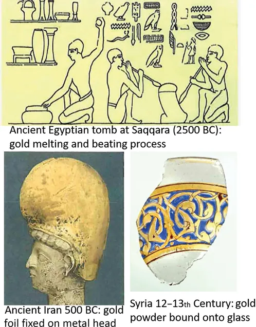
Coating technologies evolved after the Industrial Revolution as people sought better, less expensive, and long-lasting coatings. This led to the rise and development of thin film materials, which became basis for the modern coating technology. The first chemo-mechanically made inorganic thin film could be traced back to the Egyptians, who used them for beauty purposes. This coating technology was later adopted in optical applications [5]. The coating was made of several layers of gold during the Middle Bronze Age (approximately 5000 years ago) and was deposited in tombs and the pyramids owned by royal families. These gold coatings were also found on bronze statues and other religious items in Egypt. This was prompted by the availability of the minerals along the Nile and shores of the Red Sea [6]. Some of the early uses of gold coatings have been documented [4] and examples are illustrated in Figure 1.1.
FIGURE1.1 Showing gold melting and beating to form foils, leaves, or films during the ancient Egypt. Some of the uses for the gold sheath and leaves are also shown [4]. (Reused under open access licence.)
Thin film coatings were initially employed manually, where artisans practised gold sheathing, which involved the creation of a thin layer of gold strips on surfaces such as wood and bronze to increase their beauty (Figure 1.1). This art was found in areas believed to be owned by noble rulers and families in ancient Egypt, such as Queen Hetepheres and Pharaoh Tutankhamun. Moche Indians further advanced the thin film coating technique at the onset of approximately 100 BC by developing the oxidation-reduction coating method. The Indians used gold to create thin coatings on copper and other metals to increase their strength and improve functionality [3]. This technology has advanced and is currently known as electroless plating [3].
The evolution of thin film technology can also be traced back to the discovery of vacuum technology in 1640 with the invention of the barometer. This technology was essential since scientists needed cleaner surfaces to carry out the deposition of thin films. Otto von Guericke came up with a third-generation vacuum system from a piston pump in 1652, which kick-started the ‘vacuum’ journey [6]. This was followed by the discovery of electrical power, with the basis on the work of Von Guericke, who developed a system to convert mechanical energy to electrical energy in 1663 [7]. The discovery led to the rise of physical vapour deposition (PVD) towards the mid-1800 century [5]. Since then, thin film technology has been primarily adopted in semiconductor technology and the manufacture of energy devices. Among the primary applications are the manufacturing of photovoltaic cells and nanoscale elements for advanced microprocessors in electronic devices [8,9 and 10].
The discovery of thin film technology led to the innovation of the photovoltaic (PV) effect by Alexandre-Edmond in 1839. The physicist made the first-ever PV cell, which led to further discoveries in the thin film field [11]. The discovery of the vacuum cleaner was further advanced by Herman Sprengel in 1865, who came up with a more efficient vacuum pump, which allowed researchers to investigate gas discharges and sputter deposition.
Conclusively, considering the advancements in technology, the need for thin film technology has widened. Advances have also been made on the processing and development of thin film materials. Deposition (physical and chemical) has been adopted as among the significant processing method for these materials. This has increased the manufacture of thin film equipment and devices for industrial applications such as optical coatings, LEDs, hard coatings on machining tools, electrical devices, energy devices, power storage equipment, and drug delivery devices in the medical industry [12]. There lies a great future for thin film materials and technologies, and extensive research and development are critical.
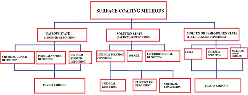
1.3 Classification of Thin Film Deposition Methods
There are so many methods of manufacturing thin film materials. These methods are classified according to the state of the ‘source’ material used in depositing thin film material. As such, these methods are classified as shown in Figure 1.2.
FIGURE1.2 Classification of surface coating/thin film deposition techniques [11]. (Reused under open access licence.)
Gaseous state,
Solution state, and
Molten or semi-molten state methods.
As shown, gaseous state deposition methods are those methods in which the source material has to be in gaseous state or has to be transformed into a gaseous state before deposition onto the substrate for condensation and formation of thin films and coatings. These methods are further classified as follows.
Physical vapour deposition,
Chemical vapour deposition, and
Ion beam–assisted deposition methods.
In PVD methods, the target (source) material is evaporated or atomised and there are no chemical reactions involved for the formation of thin film coatings. Examples of PVD methods include sputtering, thermal spray, arc vapour, ion beam, pulsed laser deposition, etc. Further details of PVD and other meth...
Table of contents
Cover
Half Title
Series Page
Title Page
Copyright Page
Dedication
Table of Contents
Preface
Acknowledgements
Authors
Chapter 1 Introduction to Thin Films and Coatings
Chapter 2 Methods of Thin Film Deposition
Chapter 3 Characterisation Techniques of Thin Films
Chapter 4 Hybrid and Scalable Thin Films
Chapter 5 Bibliometric Analysis of Applications of Thin Film Materials
Chapter 6 Thin Films for Biomedical Applications
Chapter 7 Thin Films for Surface Protection
Chapter 8 Thin Films for Cutting Tools
Chapter 9 Thin Films for Electronic, Spintronics, and Optical Applications
Chapter 10 Thin Film Materials for Energy Applications
Chapter 11 Smart and Self-Healing Thin Film Materials
Chapter 12 Thin Films for Antimicrobial Applications
Chapter 13 High Entropy Alloy Thin Films
Chapter 14 Thin Film Technology and Industry 4.0
Chapter 15 Thin Films and 3D Printing Technology
Index
Frequently asked questions
Yes, you can cancel anytime from the Subscription tab in your account settings on the Perlego website. Your subscription will stay active until the end of your current billing period. Learn how to cancel your subscription
No, books cannot be downloaded as external files, such as PDFs, for use outside of Perlego. However, you can download books within the Perlego app for offline reading on mobile or tablet. Learn how to download books offline
Perlego offers two plans: Essential and Complete
Essential is ideal for learners and professionals who enjoy exploring a wide range of subjects. Access the Essential Library with 800,000+ trusted titles and best-sellers across business, personal growth, and the humanities. Includes unlimited reading time and Standard Read Aloud voice.
Complete: Perfect for advanced learners and researchers needing full, unrestricted access. Unlock 1.5M+ books across hundreds of subjects, including academic and specialized titles. The Complete Plan also includes advanced features like Premium Read Aloud and Research Assistant.
Both plans are available with monthly, semester, or annual billing cycles.
We are an online textbook subscription service, where you can get access to an entire online library for less than the price of a single book per month. With over 1.5 million books across 990+ topics, we’ve got you covered! Learn about our mission
Look out for the read-aloud symbol on your next book to see if you can listen to it. The read-aloud tool reads text aloud for you, highlighting the text as it is being read. You can pause it, speed it up and slow it down. Learn more about Read Aloud
Yes! You can use the Perlego app on both iOS and Android devices to read anytime, anywhere — even offline. Perfect for commutes or when you’re on the go. Please note we cannot support devices running on iOS 13 and Android 7 or earlier. Learn more about using the app
Yes, you can access Thin Film Coatings by Fredrick Madaraka Mwema,Tien-Chien Jen,Lin Zhu in PDF and/or ePUB format, as well as other popular books in Technology & Engineering & Electrical Engineering & Telecommunications. We have over 1.5 million books available in our catalogue for you to explore.