![]()
1Introduction
In spintronics the intrinsic magnetic property of the electron, its spin, is used for switching purpose in an electronic circuit instead of its charge. The operation principle of spintronic devices is based on completely different physical phenomena compared to their charge-based counterparts. In this textbook, we will have a closer look at the physical mechanisms of which spintronic devices make use. The roots of spintronic devices lie in the field of magneto-electronic devices. As a matter of fact, metallic magneto-electronic devices are already well established in information technology. The basic physical phenomena are giant magnetoresistance (GMR) or tunneling magnetoresistance (TMR). These structures contain ferromagnetic layers which are either separated by a metallic layer or by a tunneling barrier, respectively. By keeping the magnetization in one layer fixed and changing the magnetization in the other one with respect to the first, the resistance is changed. This mechanism can be used for switching or detection purposes. In the meantime both effects have been implemented in applications, e.g. GMR or TMR devices are used as read heads in state-of-the-art hard disc drives and were responsible for the huge increase of storage capacity in recent years. Because of its significance the Noble prize in physics was awarded to Albert Fert and Peter Grünberg in 2007: “For the discovery of magnetoresistance” [3, 4]. The GMR and TMR effect can also be employed in solid-state memories, i.e. magnetoresistive random access memories (MRAMs). The memory cells can be programmed by changing the magnetization of one magnetic layer with respect to the other by means of a magnetic field generated by two crossing current carrying lines. More recent switching schemes use spin-transfer torque. Instead of employing an external magnetic field, here the switching is achieved by using a spin-polarized current through the memory cell itself. The advantage of magnetic memories is that they are nonvolatile, i.e. the stored information remains even after the power supply is switched off. MRAM chips are already commercially available.
So far, magnetic device structures are mainly used for data storage, while the data processing itself is performed by semiconductor devices. Here, the work horse is the field-effect transistor. The vast majority of these transistors is made from silicon as a semiconductor material. During the last decades one could observe a continuous shrinkage of device dimensions following the so-called Moore’s law [1]. This allowed the integration of more and more devices on a chip and the design of more complex circuits as well as denser solid-state memories. However, it is foreseeable that the miniaturization of Si-based circuits will reach its limits [2, 5]. Therefore, various alternative concepts are pursued, e.g. by extending the material base by using SiGe or by implementing novel device concepts like the tunnel field-effect transistor. Above that, more revolutionary concepts are also considered. One of them is semiconductor spintronics, where the electron spin is the entity, which is exploited for information processing. Using the electron spin in a device promises to perform digital switching sequences faster with less power consumption [6–11]. A prominent example of a spintronic device is the spin field-effect transistor (spin FET), proposed by Datta and Das [6]. Although the field of semiconductor spintronics has existed for some years already, these kind of devices have not yet found their way into electronic circuits. However, in the meantime a working spin FET as a demonstrator has been realized [12].
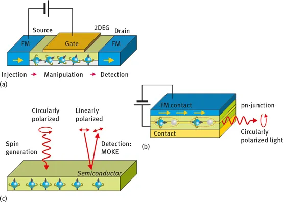
Let us have a look on different physical mechanisms employed in spintronic devices. Figure 1.1 (a) shows a schematic of a spin field-effect transistor.
Spin-polarized carriers are supplied from the ferromagnetic source contact by driving a current between source and drain. The spins are injected into the semiconductor material, keeping their initial spin polarization in the ferromagnet. As we will discuss in Chapter 6, this is a formidable task. Owing to the conductance mismatch and to imperfect interfaces, spin injection is often quite inefficient. In Chapter 4, we will introduce diluted magnetic semiconductors, which might be an interesting alternative to metallic ferromagnetic injectors, owing to their better conductance matching. Once the spin-polarized carriers are injected into the two-dimensional electron gas in the semiconductor, their spin orientation is manipulated by means of the Rashba effect [13]. Applying a voltage to the gate electrode results in a change of the electric field to which the electrons in the semiconductor are exposed. The electrons propagating in that electric field experience an effective magnetic field. The electron spin precesses about this effective magnetic field. The degree of spin precession depends on the strength of the electric field and thus on the gate voltage. The underlying physical mechanisms of a spin FET are introduced in Chapter 7. After passing the semiconductor section, the spin orientation is detected by the ferromagnetic drain contact. Ideally electrons can only enter where the spin orientation matches the magnetization in the drain contact. By biasing the gate the spin orientation of the carriers reaching the drain contact can be controlled. This is the switching scheme of the spin field-effect transistor. In an alternative concept electron interference can also be employed for switching purposes. This will be discussed in Chapter 8.
Fig. 1.1: (a) Schematic illustration of a spin field-effect transistor. Spins are injected into the two-dimensional electron gas (2DEG) in the semiconductor. The spin orientation is manipulated by biasing the gate electrode. (b) Spin light emitting diode (spin LED). Spin-polarized electrons are supplied from the top ferromagnetic electrode. The unpolarized holes are provided by the bottom contact. Electron hole recombination results in the emission of circularly polarized light. (c) Spinpolarized electrons can by generated by circularly polarized light. The spin orientation can be detected by the magnetooptical Kerr effect (MOKE). Here, the polarization direction of a reflected linearly polarized beam of light is changed in the presence of spin-polarized carriers in the semiconductor.
Owing to the inefficiency of purely electric spin injection and detection, often optical means are utilized as an alternative to measure spin-polarized carriers. A typical example is given in Figure 1.1 (b), where a spin light emitting diode (spin LED) is shown. Spin-polarized electrons are transferred from a ferromagnetic electrode into a quantum well layer. Here, the electrons recombine with unpolarized holes provided by the bottom contact. Owing to the spin polarization of the electrons, circularly polarized light is emitted. This is due to angular momentum conservation during the recombination process. Thus, the emission of circularly polarized light can be used to verify spin injection from a ferromagnetic electrode into a semiconductor. Moreover, the spin LED can also directly be used in applications, where it serves as an emitter for circularly polarized light.
One can even move one step further and perform all-optical experiments. As an inverse process, circularly polarized light can also be employed to generate spin-polarized electrons in direct band gap semiconductors. Here, spin-polarized electron-hole pairs are excited by the irradiated light. Due to strong spin orbit coupling in the valence band, the spin polarization of the holes decays quickly, while the electron spin polarization remains. This is a very efficient method to generate spin-polarized electrons, compared to electrical spin injection. The presence of spin-polarized carriers in a semiconductor can also be detected by optical means, i.e. by the magnetoopticalKerr effect (MOKE). Here, a beam of linearly polarized light is reflected at the surface. In the presence of spin-polarized carriers, the polarization of the reflected beam is rotated. The rotation angle is proportional to the magnetization in the semiconductor, and thus it can be employed as a parameter to quantify the magnetization in a semiconductor. As a matter of fact, optical means are very powerful means to generate or detect spinpolarized carriers. However, conceptually one runs into problems when it comes to miniaturization. This can be achieved much more easily by purely electrical means. Indeed, in this textbook we will mostly focus on electrical phenomena, whereas optical effects will only be covered when they serve in experiments to generate or measure spin-polarized carriers.
Recently spintronics has made a large leap towards novel phenomena and materials, such as the quantum spin Hall effect or topological insulators [14–16]. Regarding the first, the strong spin orbit coupling in a HgTe/CdTe heterostructure results in an inversion between the conduction and valence bands. As a consequence, one-dimensional channels are formed at the edge of the sample, similarly to what is known for the quantum Hall effect. The crucial difference is that these edge channels are formed at zero magnetic field, whereas in the case of the quantum Hall effect a magnetic field is required. Furthermore, the transport on the edges is spin polarized. In this sense it is related to the spin Hall effect discussed later in Chapter 9, where spin-dependent scattering of propagating electrons also results in spin-polarized carriers at the edge of the sample.
Very similar effects to the quantum spin Hall effect are observed in three-dimensional topological insulators, where due to the very strong spin orbit coupling a conductive two-dimensional surface channel is formed. This surface channel is inherently stable, i.e. topologically protected. Quantum spin Hall systems and three-dimensional topological insulators are completely new states of matter. The related physical effects have not yet been fully explored. In any case, they promise a huge potential for future spintronic devices. The properties of these materials are discussed in Chapters 10 and 11.
Apart from more conventional circuits a new scheme for information processing has emerged which is directly based on quantum mechanics. Instead of 0 and 1 as two states, a bit (cf. Figure 1.2 (a)), i.e. the smallest unit of information in a conventional computer, in quantum computing the quantum bit (qubit), is constituted by a quantum mechanical two-level system. This is illustrated in Figure 1.2 (b) [17].
The increase of computational power, e.g. for factorizing large numbers [18], originates from the fact that the corresponding algorithms make use of quantum mechanical superposition and entangled states. Spin-1/2 systems are ideally suited to realize a qubit, since the Zeeman split states naturally represent the required two-level system. In practice, this two-level system...