1.1 Introduction of Nanomaterials
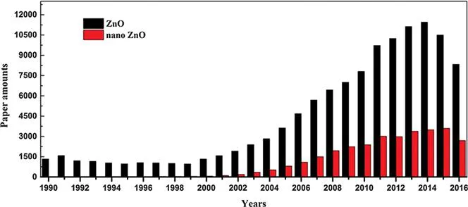
Nanoscience and nanotechnology, emerging research fields with pioneering theory and multi-disciplinary approaches, have raised wide concern since their inception. At the beginning of the 1990s, developments in physics brought revolutionary progress for small scale characterisation, as well as a novel understanding of nanosized materials. In the following decades, with an intensive study on physical and chemical properties of nanomaterials and extensive attempts at their preparation methods, nanoscience and nanotechnology have been gradually developed into the most popular frontier interdisciplinary subject. Their research content involves physics, chemistry, materials science, mechanics, microelectronics, biology, medical science and many other related subjects. More recently, the rapid development of nanoscience and nanotechnology have created great influences on social economy development science and technology advancement as well as daily life (Figure 1.1).
Figure 1.1 Statistics on ZnO-related published papers from 1990 to 2016.
Since the beginning of the new century, European countries and the USA have successively launched various development programs focused on nanoscience and nanotechnology,1–3 especially the National Nanotechnology Initiative (NNI) proposed by the USA, which raised the nanotechnology development to national strategy level. In 2006, the National Long-term Scientific and Technological Development Plan (2006–2020) issued by China has firmly claimed ‘nanoresearch’ as a key program for basic research and identified nanoscience and nanotechnology advancement as a state major development policy on science and technology. China’s Energy Development Strategy Action Plan (2014–2020) also listed micro-nano new energy as one of the nine key fields of innovation. The NASA 2015 technology roadmap also pointed out that nanotechnology was a necessary technical requirement to achieving NASA’s goals in science, human exploration and science missions for the next 20 years.
Low dimensional functional nanomaterials remain a worldwide hot spot. They are ideal structural units for constructing functional nanodevices because of their special properties, and always lead to outstanding performance in multi-subject fields like energy, information, environment, microelectronics, biology, medicine, national defence, etc. Their family includes advanced carbon nanomaterials, traditional single element semiconducting nanomaterials, metal nanomaterials, and organic nanomaterials, as well as emerging oxide semiconducting nanomaterials, etc., which generally present excellent and unique mechanical, optical, electrical, thermal acoustic, magnetic properties that bulk materials do not have.4–16 This is the essential foundation for the development of nanoscience and nanotechnology.
People have experienced a long-lasting period of investigating nanomaterials and nanotechnology. In the early of 20th century, Wilhelm Ostwald, the owner of the Nobel Prize in Chemistry and known as the father of physical chemistry, stated in his ‘The World of Neglected Dimensions’ that people had realised the importance of the mesoscopic field. The so-called ‘mesoscopic’ means the state between microscopic and macroscopic, namely the scale between nanometre and millimetre.17 The conception of nanoscience and nanotechnology was first proposed by Richard Feynman in his speech at Caltech in 1959. After nearly 100 years of exploration until around 1990, along with the development of science and technology, the great breakthrough made particularly in terms of mesoscopic scale characterisation approaches, and great quantities of invented nanoscale characterisation facilities, such as transmission electron microscope (TEM), scanning electron microscope (SEM), scanning probe microscope (SPM), etc., meant that people had truly entered the nanoworld.
The development process of nanomaterials can be divided into three stages: in the first stage (before 1990s), research was mainly focused on nanometre particles, such as nanometre crystalline, nanometre phase, nanometre amorphous as well as their characterisation methods and evaluation methods for their unique properties. In the second stage (1990–1994), research mainly concentrated on controllable synthesis for certain morphologies to acquire peculiar physical and chemical properties that originated from nanometre materials. Especially, exploration on synthesising the nanocomposites gradually became the main direction. In the third stage (1994–present), nanostructure assembling systems, or so-called nanoscale patterned materials, started to draw researchers’ attentions. Based on the basic units like nanoparticles, nanowires and nanotubes, various complex nanostructures in one-, two- and three-dimensions, were successfully assembled. The third stage focused on designing, assembling and developing novel systems according to researchers’ will, thereby realising the expected certain properties. For now, booming nanoscience and nanotechnology have stepped into a new era, where the modulation of structures and properties of nanomaterials have already tended to be developed and the nanomaterial based functional devices have already been realised for preliminary applications.
1.2 Introduction of ZnO Nanomaterials
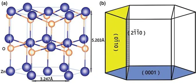
The detailed physical property parameters of ZnO are as follows: the relative molecular mass is 81.37 g mol−1, the density is 5.67 g cm−3, the surface work function is 5.3 eV, the melting point of bulk ZnO material is 1975 °C, and the boiling point is 2360 °C. ZnO belongs to wurtzite, with a hexagonal crystal structure, and the space group is P63mc. The crystal lattice constants of ZnO are: a=3.2496 Å and c=5.2064 Å, and the actual measurement of these are: a=3.24–3.26 Å and c=5.13–5.43 Å.8,18–20
The structure of ZnO can simply be described as follows: countless closely packing O2− and Zn2+ layers alternately stacked in the direction of the c axis, with the adjacent layers of O2− and Zn2+ forming a tetrahedral structure. The structure of ZnO described in different ways is shown in Figure 1.2. The tetrahedral structure of ZnO is the intrinsic cause of its non-centrosymmetrical characteristic, which directly leads to its piezoelectric effect and thermoelectric effect.21
Figure 1.2 The ZnO crystal structure.
ZnO, a typical direct wide band gap semiconducting material (3.37 eV at room temperature) with piezoelectric and photoelectric characteristic, is similar to gallium nitride (GaN). In its energy band structure, the bottom of the conduction band (CB) is formed essentially from the 4s level of Zn2+ and antibonding sp3 hybrid states, and the top of valence band (VB) from the occupied 2p orbits of O2− or from the bonding sp3 orbitals.22,23 At room temperature, the defect level such as donor level and acceptor level are mainly distributed in the forbidden band of ZnO ranging from ∼0.05 to 2.8 eV, and the band gap of ZnO is 3.4 eV. Besides, ZnO possesses a large exciton binding energy of 60 meV, which is much larger that of zinc selenide (ZnSe) (22 meV) and GaN (25 meV), and thus it is promising for various applications.
ZnO has unique electrical and thermal properties, as well as chemical stability. As a short-wave light-emitting material, its high stability demonstrates an enormous utility value. The traditional synthesis technology could hardly acquire favourable single crystal or thin film ZnO, which restricted its application as a light-emitting material. In recent years, with the development of synthesis approaches, the above-mentioned problem was gradually solved. Ever since people discovered the phenomenon of optical pumping simulated emission at near ultraviolet (UV) of thin film ZnO, it has played a very important role in improving optical recording density and the access speed of optical information due to the shorter wave length in the near UV photoluminescence of ZnO than the blue light emission of GaN. It is also expected to realise breakthrough results for application aspects such as surface acoustic wave, transparent electrode, optoelectronic devices and blue light emitting devices.
Various superior physical characteristics of ZnO make it widely adopted in the field of rubbers, ceramics, coatings and optoelectronics. At present, the research on photocatalytic performance for organic waste degradation and disinfection has been applied in practical waste water treatment; the research on UV absorption performance has been applied for anti-UV agents in textiles and cosmetics. In addition, the wide application prospects in the fields of photoelectric conversion, sensors, nanoelectro-mechanical systems, field emission devices and nanometre lasers have also been highlighted. Notably, the nanogenerator was invented by taking advantage of the piezoelectric effect of ZnO.24–26
In terms of morphology and scale size, ZnO nanomaterials can be divided into three types including zero-dimensional materials (ZnO nanoparticles), one-dimensional materials (ZnO nanorods, na...