![]()
Chapter 1
Introduction
1.1. Historical Developments
The semiconductor optical amplifier (SOA) is very similar to a semiconductor laser. The laser has a gain medium and an optical feedback mechanism. The latter is generally provided by the cleaved facets of the semiconductor itself or by a grating of suitable periodicity etched close to the gain medium. At threshold, the gain equal loss for a laser, and the gain needed for laser action is typically ~5 to 10dB. A traveling wave optical amplifier has only a gain medium. However, the gain is generally larger (~20 to 25 dB) compared to that for a laser. The optical gain is caused by the recombination of electrons and holes (electrons and holes are injected by external current). Thus the semiconductor amplifier operates at a higher current density than a laser at threshold.
The concept of the laser dates back to 1958 [1]. The successful demonstration of a solid state ruby laser and He-Ne gas laser was reported in 1960 [2,3]. Laser action in semiconductor was considered by many groups during that period [4–6]. The semiconductor injection laser was demonstrated in 1962 [7–10]. CW operation of semiconductor laser was demonstrated in 1970 [11,12] using the concept of double heterostructure [13]. Since then the semiconductor injection laser has emerged as an important device in many optoelectronic systems such as optical recording, high-speed data transmission through fibers, optical sensors, high-speed printing, and guided wave signal processing. An important impact of semiconductor lasers is in the area of fiber optic transmission systems where the information is sent through encoded light beams propagating in glass fibers. These lightwave transmission systems, which have been installed throughout the world, offer a much higher transmission capacity at a lower cost than coaxial copper cable transmission systems.
The advantages of semiconductor lasers over other types of lasers, such as gas lasers, dye lasers, and solid-state lasers, lie in their considerably smaller size and lower cost and their unique ability to be modulated at gigahertz speeds simply by modulation of the injection current. These properties make the laser diode an ideal device as a source in several optoelectronic systems, especially optical fiber transmission systems. Semiconductor laser properties are discussed in several books [14–17]
Historically, the research on optical amplifier followed that of the semiconductor laser. Early work was carried out using GaAs/AlGaAs material system [18–21]. A majority of the follow-on work has been using the InGaAsP/InP material system. This material system is suitable for producing amplifiers with optical gain in the 1300 to 1600 nm wavelength range. The fiber optic transmission systems operate in this wavelength range due to the low loss of optical fibers and the commercial application of optical amplifiers are going to be driven by their need in fiber communication systems. This book provides a comprehensive and detailed account of design, fabrication, and performance of SOAs in optical networks. Earlier work is discussed in previous books [22,23].
1.2. Semiconductor Materials
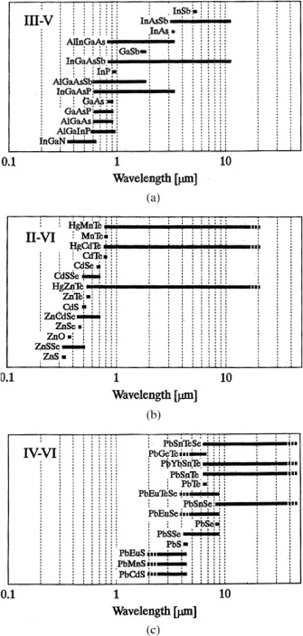
The choice of materials for semiconductor amplifiers is principally determined by the requirement that the probability of radiative recombination should be sufficiently high that there is enough gain at low current. This is usually satisfied for “direct gap” semiconductors. The various semiconductor material systems along with their range of emission wavelengths are shown in Fig. 1.2.1. Many of these material systems are ternary (three-element) and quaternary (four-element) crystalline alloys that can be grown lattice-matched over a binary substrate.
Many of these materials were first used to make semiconductor lasers [7–10, 14–17]. The lines represent the range of band gaps can be obtained by varying the composition (fraction of the constituting elements) of the material. The optical gain in amplifiers occurs at wavelengths close to the band gap. Thus a suitable set of materials must be chosen to get optical gain at the desired wavelength.
Fig. 1.2.1. Semiconductor materials used in laser fabrication at different regions of the spectrum. The three figures refer to compound semiconductors formed using group III and group V elements (III-V), group II and group VI elements (II-VI) and group IV and group VI elements (IV-VI) of the periodic table [24]. The quantum cascade lasers are fabricated using III-V semiconductors and they operate on intraband transitions in a quantum well.
Another important criterion in selecting the semiconductor material for a specific heterostructure design is related to lattice matching i.e. the crystalline materials that form the heterostructure must have lattice constants which are equal to within ~0.01 %. The binary substrates that are commonly used are GaAs and InP. They can be grown in a single crystal form from a melt. The ternary or quaternary semiconductors are epitaxially grown over the binary substrate for semiconductor laser or amplifier fabrication. In the epitaxial growth process the single crystal nature is preserved across the interface of the two materials. This leads to near absence of defect sites at the interface.
The development of epitaxial growth techniques has been of major significance for the development of semiconductor photonic devices such as lasers, amplifiers, and, photodetectors. The commonly used techniques for epitaxial growth are liquid phase epitaxy (LPE) [25], vapor-phase epitaxy (VPE) [26], molecular beam epitaxy (MBE) [27], and metal organic chemical vapor deposition (MOCVD) [28]. Early work on lasers and amplifiers were carried out using the LPE growth technique. The MBE technique is very useful for the growth of very thin semiconductor layers and was first used to fabricate quantum well structures [29]. The MOCVD technique and its variants are generally used for commercial production of lasers, amplifier and photodetectors. These growth techniques are described in detail in Ch. 4. In addition to growth, processing techniques of semiconductor materials for laser or amplifier fabrication was developed. The processing techniques include current confinement, low resistance contacts and etching of the semiconductor material to form specific geometries [33–35].
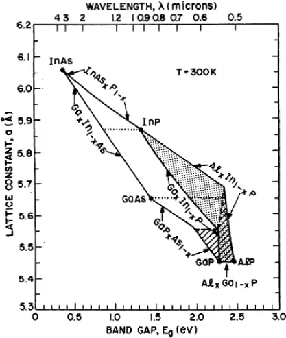
In the absence of lattice match, the quality of the hetero-interface is poor, i.e. there are lattice defects which serve as non-radiative recombination sites. In certain instances it is possible to grow epitaxially thin layers of one semiconductor on top of another in the presence of a lattice mismatch of few percent. Such growth is called strained layer epitaxy, it is discussed in Sec. 4.4. Figure 1.2.2 shows the relationship between band gap Eg and lattices constant a of several ternary compound semiconductors. The dots correspond to the binary compounds and the lines represent the ternary compounds.
Fig. 1.2.2. Band gap and lattices constants of several ternary and quaternary compounds formed from the binary compounds. For In1-xGaxAsyP1−y quaternary material, the clear region is the region of direct band gap [2].
The ternary semiconductor AlxGa1-x As can be grown over a GaAs substrate over the entire range of Al fractionxbecause GaAs and AlAs have nearly the same lattice constant. However, the AlxGa1-x As material has a direct band gap for compositions with x < 0.45. Semiconductors with direct band gap are needed for efficient light emission. Heterostructures using the AlGaAs/GaAs material system was the first to be studied extensively. Semiconductor lasers, amplifiers, bipolar transistors, field effect transistors have been made using this material system.
In the 1970’s, considerable resources were devoted for lasers and photodetector fabrication using the quaternary In1-xGaxAsyP1-y/ InP material system. This material system is particularly suitable for lasers in the ~1.3 to 1.55 μm wavelength range which is the region of low dispersion and low optical loss for silica optical fibers. In1-xGaxAsyP1-y can be grown lattice matched over a InP single crystalline substrate for In1-xGaxAsyP1-y compositions for which x ~ 0.45y. Lasers and detectors based on this material system are widely used in current fiber optic communication systems. Semiconductor amplifiers are important for all-optical networks which operate near 1.55 μm wavelength range. Thus much of the developments on optical amplifiers in the 1990’s and continuing on has been using the In1-xGaxAsyP1-y /InP material system.
1.3. Operating Principles
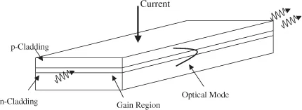
SOA is very similar to a laser except it has no reflecting facets [36,37]. A typical amplifier chip is ~0.6 to 2 mm long. It has a p-cladding layer, a n-cladding layer and a gain region all of which are epitaxially grown over a binary substrate.
The schematic of a SOA chip is shown in Fig. 1.3.1. The amplifier chips have cleaved facets with anti-reflection coating (and possibly other modifications) which reduce its reflectivity to nearly zero. Just like the laser, the amplifier has a p-n junction which is forward biased during operation. The injected current produces gain in the gain region.
Fig. 1.3.1. Schematic of a SOA with no waveguide in the lateral (along the plane of p-n junction) direction.
The majority carries are holes in the p-cladding layer and they are electrons in the n-cladding layers. The electrons and holes are injected into the gain region which is made of a lower band gap semiconductor than the cladding layers. The co-located electrons and holes recombine. This results in spontaneous emission of light and optical gain for light propagating in the gain region. It is a fortunate coincidence that semiconductor with lower band gap also has a higher index than semiconductors with higher band gap. The small index difference produces a waveguide for the propagating signal light. The signal is guided in this waveguide and it experiences amplification (gain) until it emerges from the output facet of the amplifier. Thus the double heterostructure ...