![]()
Lecture 1
Overview
Contents
1.1 Introduction
1.2 Diffusive electron transport
1.3 Types of electron transport
1.4 Why study near-equilibrium transport?
1.5 About these lectures
1.6 Summary
1.7 References
1.1 Introduction
This short set of lectures is about how electrons in semiconductors and metals flow in response to driving forces such as applied voltages and differences in temperature. The simplest description of transport is the famous Ohm’s Law (Georg Ohm, 1927),
(1.1)
which states that the current through a conductor is proportional to the voltage across it. One goal of these lectures is to develop an understanding of why and under what conditions the current-voltage characteristic is linear and to understand how the resistance is related to the material properties of the resistor. Before launching into the lectures, let’s spend a few minutes discussing what the following lectures are all about.
1.2 Diffusive electron transport
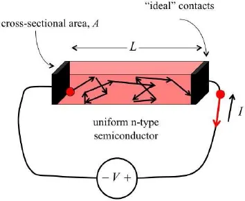
The transport of charge carriers such as electrons is a rich and deep field of physics. While we won’t be delving into the underlying physics in great detail, it will be necessary to have a firm grasp of some fundamentals. Consider Fig. (1.1), which illustrates diffusive electron transport in a simple resistor (made with an n-type semiconductor for which the current is carried by electrons in the conduction band).
Fig. 1.1. Illustration of diffusive electron transport in an n-type semiconductor under bias.
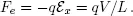
Because the positive voltage on the right contact attracts electrons, they tend to flow from left to right, but it is a random walk during which electrons frequently scatter from defects, impurities, etc. In the traditional approach, we say that electrons feel a force due to the electric field,
(1.2)
The electric field accelerates electrons, but scattering produces an opposing force, so the result is that in the presence of an electric field, electrons drift at a steady-state velocity of
(1.3)
where µn is the mobility, a material-dependent parameter.
We obtain the current by noting that it is proportional to the charge on an electron, q, the density of electrons per unit volume, n, the crosssectional area, A, and to the drift velocity, υd. The current can be written as
(1.4)
where
(1.5)
with G being the conductance in Siemens (S = 1/Ohms), and σn the conductivity in S/m (1/Ohm-m). Equation (1.4) is a classic result that we shall try to understand more deeply.
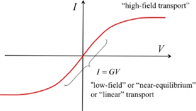
Figure (1.2) is a sketch of what a measured I – V characteristic might look like for a semiconductor like silicon. We see that there is a region for which the current varies linearly with voltage. (This is the regime of near-equilibrium, linear, or low-field transport that we shall be concerned with. Under high bias, the current becomes a non-linear function of voltage (and may even be non-monotonic, as in semiconductors like GaAs). A proper discussion of high-field transport would require another set of lecture notes. The interested reader can consult Chapter 7 of Lundstrom [1].
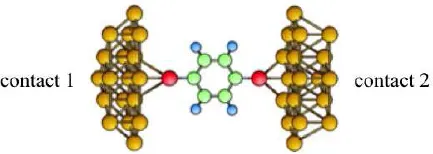
Figure (1.3) illustrates the kind of problem that engineers and applied scientists are increasingly dealing with — an extremely short conductor, in this case a small molecule. The resistance of devices like this can be measured, and we need a theory to understand the measured resistance. Equation (1.4), seems ill-suited to this problem, but a general transport theory should be able to treat both large conductors and very small ones. When we develop this theory, we will find some surprises. For example, we’ll find that there is an upper limit to the conductance, no matter how short the conductor is and that conductance comes in quantized units. These facts are well-known from research on mesoscopic physics (e.g. see Datta [2]) but they have now become important in device research and engineering.
Fig. 1.2. Illustration of a typical current vs. voltage characteristic for a semiconductor like silicon.
Fig. 1.3. Illustration of a small organic molecule (phenyl dithiol) attached to two gold contacts. The I – V characteristics of small molecules can now be measured experimentally. See, for example, L. Venkataraman, J. E. Klare, C. Nuckolls, M. S. Hybertsen, and M. L. Steigerwald, “Dependence of single-molecule junction conductance on molecular conformation”, Nature, 442, 904-907, 2006.
1.3 Types of electron transport
Electronic transport is a rich and complex field. Some important types of transport are:
(1) near-equilibrium transport
(2) high-field (or hot carrier) transport
(3) non-local transport in small devices
(4) quantum transport
(5) transport in random/disordered/nanostructured materials
(6) phonon transport
Near-equilibrium transport is diffusive in conductors that are many mean-free-paths long, but it is ballistic when the conductor is much shorter than a mean-free-path. We shall discuss both cases. High field transport in bulk semiconductors is also diffusive, but since the carriers gain significant kinetic energy from the high electric field, they are more energetic (hotter) than the lattice. Under high applied biases, the current is a nonlinear function of the applied voltage, and Ohm’s Law no longer holds. (See Chapter 7 of Lundstrom [1] for a discussion of high field transport.)
In modern semiconductor devices, modest applied biases (e.g. 1 V) can produce large electric fields across the short, active regions. Under these conditions, carrier transport becomes a nonlocal function of the electric field, and interesting effects such as velocity overshoot can occur. (See Chapter 8 of Lundstrom [1] for a discussion of these effects.) Finally, as devices get very short and the potential changes rapidly on the scale of the electron’s wavelength, effects like quantum mechanical reflection and tunneling become important. For an introduction to the field of quantum tranport, see Datta [3].
Another important class of problems has to do with transport in various kinds of disordered materials. Much of traditional transport theory assumes a periodic crystal lattice and makes use of concepts like crystal momentum and Brillouin zones. In these lectures, we will restrict our attention to this class of problems. Amorphous materials, however, do not possess long range order; some interesting new features occur, but many of the essential aspects of scattering are similar (e.g. see Mott and Davis [4]). Polycrystalline materials consist of single crystal grains separated by grain boundaries. The statistical distributions of grain sizes, orientations, and grain boundary properties complicate the description of electron transport. Indeed, much of the promise of nanotechnology lies in the hope that artificially structuring matter at the nanoscale will provide properties not found in nature. We believe that the approach used in these lectures will prove useful for this class of problems as well, but this is a topic of current research, and the lecture notes volume will have to wait.
Finally, we should mention that although our attention in these lectures is on electron transport in semiconductors and metals. Phonon transport is also important, and many of the concepts developed to describe electron transport can just as well describe phonon transport. The calculation of the thermal conductivity is ...