![]()
Chapter 1
System Integration and Modeling Concepts
The semiconductor industry has come a long way since Dr. Gordon E. Moore, co-founder of Intel, formulated his empirical law called Moore’s law in 1965, almost five decades back. Today, Moore’s law is being used by the semiconductor industry for research and planning purposes and has been the primary driver for having more than a billion transistors in an integrated circuit chip today. Over the last two decades, the packaging industry has followed Moore’s law but more at the System’s level where the focus has been on system miniaturization rather than on IC integration, with the coining of the phrase “More than Moore” leading to the development of System in Package (SIP) and System on Package (SOP) technologies. So, what comes next both in the near and distant future? In this chapter we provide an introduction to IC and System Integration and paint a vision for the future with a primary focus on System Integration using packaging as a platform for integration. Since, the next semiconductor wave is 3D integration, which is also the focus of this book, we discuss the packaging aspects with a focus on interposer based solutions.
A very important part of this chapter is on the need for modeling and simulation to maximize performance. With 3D integration still in its infancy at the time of writing this book, we discuss some introductory aspects to modeling with details covered in the rest of the chapters of this book.
1.1Moore’s Law
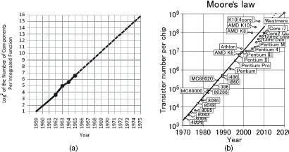
Dr. Gordon E. Moore was awarded the IEEE Medal of Honor in 2008 for “pioneering technical roles in integrated circuit processing, and leadership in the development of MOS memory, the microprocessor computer and the semiconductor industry”, an apt recognition to a person who has helped shape the semiconductor industry. In 1965, Dr. Moore predicted that the number of components per integrated circuit (IC) in the future will double every year based on a few data points as shown in Figure 1.1(a) [Moore, 1965]. In 1975, Dr. Moore altered his prediction to the doubling of transistors per IC every two years based on additional data points. Coined as Moore’s law around 1970 by Dr. Carver Mead, a professor at Caltech, this law has been the primary driver for the semiconductor industry over the last several decades. Moore’s law today is attributed to the doubling of transistors every 18 months and has led to more than a billion transistors on a single chip, as shown in Figure 1.1(b).
As we all know today, packing more transistors in an IC requires fine line lithography, which enables the scaling of the transistor. Interestingly enough, Dr. Moore never indicated anywhere that scaling the transistor would result in a better performing transistor, a concept that was derived later. Today, we know that packing more transistors per unit area (increasing transistor density) leads to better performance, with higher functionality made possible due to the availability of more transistors in the IC. Though empirical, Moore’s law has helped shape and drive the semiconductor industry. In 2008, Dr. Moore was featured on the cover of IEEE Spectrum Magazine [Perry, 2008] where he was asked “What would you like your legacy to the world to be” to which he replied “Anything, but Moore’s law”!
Figure 1.1: (a) Dr. Moore’s original prediction in 1965 (components/IC doubling every year) [Moore, 1965] and (b) transistor count in a microprocessor Vs year of introduction.
1.2IC Integration Vs System Integration – What is the Difference?
Over the last four decades the size of systems has reduced exponentially while the functionality that they support has increased dramatically.
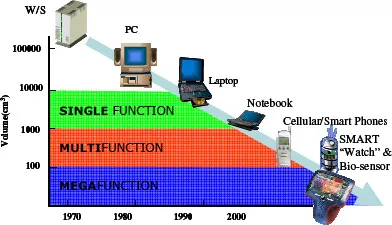
This is depicted in Figure 1.2 where the first modern workstations, also called mini computers, introduced by Xerox Palo Alto Research Center (PARC) in 1973 called Xerox Alto were single-user machines with high-resolution graphics and mouse driven graphical user interface. In the late 1970s, minicomputers led to the modern microcomputers with Commodore PET, Apple II and TRS-80 by Radio Shack being introduced in 1977. By 2008, the number of personal computers in use world wide hit 1 billion. Personal computers were desktop computers as opposed to the workstations, where a significant cost reduction led to their usage as a home computer. In the mid 1990s, the modern mobile computers became popular due to the need for portability and lapability, a term meaning the resting of the computer on a person’s lap which doesn’t exist in the English dictionary. Though subtle in differentiation, the laptops led to notebooks in the mid 2000s through significant weight reduction using a smaller battery, a smaller screen, ultra thin profile, smaller keyboard, removal of the internal floppy drive and with an integrated modem for network connection. Though portable computers have become popular over the last decade, the first portable computer was introduced in 1981 by Adam Osborne, an ex-book publisher. Called as the Osborne 1, it weighed 24 pounds and cost $1795. Along with portability, laptop and notebook computers enabled mobility through the advent of wireless communication for consumer applications in the 1990s, which allowed users to stay connected anywhere in the world. A natural extension of mobility for data through portable computers was voice communication through the introduction of the first commercial cell phone in 1983 by Motorola. Called as DynaTAC 8000x, it had a size of around 19.5cm × 4cm × 8cm, an antenna size of 20cm, an approximate weight of 1.18kg, offered 30 minutes of talk time, had a storage capacity of 30 numbers and cost $3,995. Needless to say, the cell phones have significantly evolved since 1983 where the smart phones of today are mobile, multimedia devices rather than verbal communication tools. The smart phones today are used for surfing the web, checking emails, taking photographs, managing our social status, listening to music, and sometimes for voice communication. As depicted in Figure 1.2, it is interesting to see the evolution of these consumer systems over the last five decades starting with the workstations which were large and bulky to the smart phones of today that are small, light weight and have multi media functionality far greater than what the workstations could support in the 1970s. The multi-function shown in Figure 1.2 refers to voice, video, email, music, internet and other multi media capability available in smart phones today as compared to the workstations that primarily focused on computing in the 1970s. Moving forward, the size of systems will continue to reduce while the functionality supported will only increase, leading to systems with mega-functions. Examples include smart watches and bio-sensor pills that have started appearing in the market today. Given the trend in system miniaturization shown in Figure 1.2, an important question to ask ourselves is: What technologies enable system miniaturization? Are these technologies purely IC driven based on Moore’s law or does packaging play a significant role as well? To answer this question, let’s compare and contrast the size reduction achieved through IC and package level integration since the 1970s.
Figure 1.2: System Miniaturization Trend (Courtesy: Prof. Rao Tummala, Packaging Research Center, Georgia Tech).
Similar to transistor count for IC integration, a measure for package level integration is the component density per square centimeter achievable outside of the IC in the package and printed circuit board. These include the voltage regulator module, interconnections, resistors, capacitors, inductors, substrates, heat sink and other peripheral components outside of the IC required to build a system. Clearly, unless these components are miniaturized, the system as a whole can never be made small and therefore system miniaturization requires both IC and package level integration.
1.3History of Integration – An Overview
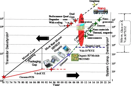
A qualitative assessment and comparison of the evolution of IC and Package level integration is depicted in Figure 1.3. To use the same metric, the transistor density and system component density per square centimeter have been used along the two vertical axes. Driven by computing and Moore’s law, the transistor density (shown on the left vertical axis) has increased, made possible by a reduction in the feature size from 10μm used by Intel in 1971 for the 4004 processor to 90nm used in 2002 by Intel for their Pentium M processor.
The world’s first single chip microprocessor in 1971 contained 2300 transistors and measured 3mm × 4mm, leading to a density of around 19000 transistors/cm2. With the usage of dip packages in the early 1970s, the packing density was limited by the pitch of the plated through holes and the line width in the printed circuit board. With a via pitch of 2.5mm, line width of 0.25mm and one line per channel [Tummala et al., 1989], an interconnection density of ~8 lines/cm2 using two wiring layers (taken as a minimum set for orthogonal wiring) was possible. Given that the printed circuit boards are used primarily for connecting ICs to each other, this routing density ultimately determined the size of the system, and is therefore referred to as system component density along the right vertical axis in Figure 1.3 (two different scales have been used for the two vertical axes). With these two data points, the ratio of IC to package level integration was roughly around 2000:1.
Figure 1.3: Integration trend (Source: Interconnect and Packaging Center, Georgia Tech, Packaging Research Center, Georgia Tech and IEEE Spectrum).
Over the next two decades until the early 1990s, the IC integration continued to increase driven by Moore’s law while the printed circuit board line widths reduced at the rate of 0.05mm every five years with a dimension of 0.05mm with 6 lines per channel between plated through hole vias on a 2.5mm pitch, translating to an interconnection density of ~48 lines/cm2 for two wiring layers. During this period dip packages were replaced by Quad Flat Pack (QFP) packages due to the higher I/O count for the die finally leading to Ball Grid Array (BGA) flip chip packages. In 1990 the Intel 80386 microprocessor was introduced with a transistor count of 275,000 in a chip of size 104mm2 leading to a transistor density of ~265,000 transistors/cm2. This translates to a ratio of around 5000:1 between transistor and system component density. With Moore’s law continuing to drive IC integration, in 1998 Intel introduced the Pentium III with a transistor count of roughly 28.1M and die size of 107mm2 while the interconnection density in the printed circuit board (2nd level package) continued to stagnate, causing a huge packaging gap (as shown in Figure 1.3) where the ratio of IC to package level integration grew to more than 0.5M:1. Though BGA packages helped reduce the package size, being single chip packages, the system size was limited by the printed circuit board routing density. Hence, several layers in the printed circuit board were necessary to complete all of the wiring to support the system functionality, or in other words, tiny ICs lead to bulky systems. In the late 1980s and early 1990s, IBM’s Multichip Module (MCM) technology was prevalent where ceramic substrates were used to connect hundreds of bipolar chips together for mainframe applications. Though this technology helped with a small reduction in the packaging gap, with the transition from bipolar to CMOS technology by IBM for CPUs in the early 1990s, integration levels within the IC increased further.
A comparison of PCB and ceramic substrate technology is shown in Table 1.1 where from the line width and line spacing, the wiring density achievable for two layers is similar for both technologies. The two main advantages of ceramic substrate over PCB wiring were its smaller layer thickness and lower loss tangent, which led to thinner modules and higher performance, respectively.
It is interesting to note that though the semiconductor industry reached a bottleneck around 2004 as shown in Figure 1.3 where scaling beyond 90nm caused significant power leakage, architectural innovations were used to solve these problems through the introduction of the dual core and multi core processors. Hence, the semiconductor industry continued to scale beyond the 90nm to 65nm and below. Since transistor scaling represents the backbone of the semiconductor industry and is required for miniaturization and performance, this can never stop and it is expected that every time the semiconductor industry hits a road block, innovations wil...