Please click here for information on Set 1: Thermal Packaging Techniques
Thermal and mechanical packaging — the enabling technologies for the physical implementation of electronic systems — are responsible for much of the progress in miniaturization, reliability, and functional density achieved by electronic, microelectronic, and nanoelectronic products during the past 50 years. The inherent inefficiency of electronic devices and their sensitivity to heat have placed thermal packaging on the critical path of nearly every product development effort in traditional, as well as emerging, electronic product categories.
Successful thermal packaging is the key differentiator in electronic products, as diverse as supercomputers and cell phones, and continues to be of pivotal importance in the refinement of traditional products and in the development of products for new applications. The Encyclopedia of Thermal Packaging, compiled in four multi-volume sets ( Set 1: Thermal Packaging Techniques, Set 2: Thermal Packaging Tools, Set 3: Thermal Packaging Applications, and Set 4: Thermal Packaging Configurations ) will provide a comprehensive, one-stop treatment of the techniques, tools, applications, and configurations of electronic thermal packaging. Each of the author-written sets presents the accumulated wisdom and shared perspectives of a few luminaries in the thermal management of electronics.
Set 2: Thermal Packaging Tools
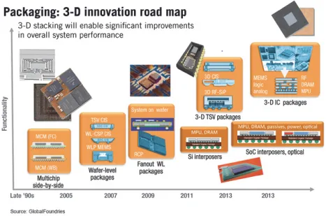
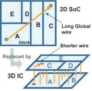
The second set in the encyclopedia, Thermal Packaging Tools, includes volumes dedicated to thermal design of data centers, techniques and models for the design and optimization of heat sinks, the development and use of reduced-order “compact” thermal models of electronic components, a database of critical material thermal properties, and a comprehensive exploration of thermally-informed electronic design. The numerical and analytical techniques described in these volumes are among the primary tools used by thermal packaging practitioners and researchers to accelerate product and system development and achieve “correct by design” thermal packaging solutions.
The four sets in the Encyclopedia of Thermal Packaging will provide the novice and student with a complete reference for a quick ascent on the thermal packaging “learning curve,” the practitioner with a validated set of techniques and tools to face every challenge, and researchers with a clear definition of the state-of-the-art and emerging needs to guide their future efforts. This encyclopedia will, thus, be of great interest to packaging engineers, electronic product development engineers, and product managers, as well as to researchers in thermal management of electronic and photonic components and systems, and most beneficial to undergraduate and graduate students studying mechanical, electrical, and electronic engineering.
Foreword
Foreword (English) (42 KB)
Foreword (Japanese) (342 KB)
Please click here for information on Set 1: Thermal Packaging Techniques
Thermal and mechanical packaging — the enabling technologies for the physical implementation of electronic systems — are responsible for much of the progress in miniaturization, reliability, and functional density achieved by electronic, microelectronic, and nanoelectronic products during the past 50 years. The inherent inefficiency of electronic devices and their sensitivity to heat have placed thermal packaging on the critical path of nearly every product development effort in traditional, as well as emerging, electronic product categories.
Successful thermal packaging is the key differentiator in electronic products, as diverse as supercomputers and cell phones, and continues to be of pivotal importance in the refinement of traditional products and in the development of products for new applications. The Encyclopedia of Thermal Packaging, compiled in four multi-volume sets ( Set 1: Thermal Packaging Techniques, Set 2: Thermal Packaging Tools, Set 3: Thermal Packaging Applications, and Set 4: Thermal Packaging Configurations ) will provide a comprehensive, one-stop treatment of the techniques, tools, applications, and configurations of electronic thermal packaging. Each of the author-written sets presents the accumulated wisdom and shared perspectives of a few luminaries in the thermal management of electronics.
Set 2: Thermal Packaging Tools
The second set in the encyclopedia, Thermal Packaging Tools, includes volumes dedicated to thermal design of data centers, techniques and models for the design and optimization of heat sinks, the development and use of reduced-order “compact” thermal models of electronic components, a database of critical material thermal properties, and a comprehensive exploration of thermally-informed electronic design. The numerical and analytical techniques described in these volumes are among the primary tools used by thermal packaging practitioners and researchers to accelerate product and system development and achieve “correct by design” thermal packaging solutions.
The four sets in the Encyclopedia of Thermal Packaging will provide the novice and student with a complete reference for a quick ascent on the thermal packaging “learning curve,” the practitioner with a validated set of techniques and tools to face every challenge, and researchers with a clear definition of the state-of-the-art and emerging needs to guide their future efforts. This encyclopedia will, thus, be of great interest to packaging engineers, electronic product development engineers, and product managers, as well as to researchers in thermal management of electronic and photonic components and systems, and most beneficial to undergraduate and graduate students studying mechanical, electrical, and electronic engineering.
Foreword
Foreword (English) (42 KB)
Foreword (Japanese) (342 KB)
Readership: Packaging engineers, electronic product development engineers, and product managers, as well as researchers in thermal management of electronic and photonic components and systems, and most beneficial to undergraduate and graduate students studying mechanical, electrical, and electronic engineering. Key Features: