![]()
Chapter 1
Introduction to Scanning
Probe Microscopy
Today’s research laboratory is required to solve difficult problems that span multiple disciplines. Advanced techniques are required to answer pressing questions related to adhesion, bonding, contamination and surface cleanliness, corrosion, surface morphology, surface roughness, surface topography, failure analysis, process monitoring, surface chemistry, biological characterization, local surface properties — both electrical and mechanical, and thin film analysis. Rarely can one analytical technique effectively span such a wide range of applications. The rapid rise of scanning probe microscopy (SPM) provides a truly marvelous tool that provides useful information about all these topics and many more.
Few scientific instruments have received as much attention and enjoyed such rapid growth as the atomic force microscope (AFM). The inherent simplicity of the AFM coupled with its ability to apply nanoNewton forces to surfaces with sub-nanometer lateral precision have led to a significant expansion in both the scope and context of the instrument. Originally used to probe the atomic roughness of a surface, the AFM has quickly evolved into a probe of surface forces using primarily only two modes of operation (contact and dynamic). Of particular significance are the rapidly evolving techniques that allow quantitative material property maps of surfaces with nanometer-scale resolution. Furthermore, the ability to position and precisely move a biased tip has been exploited to demonstrate novel nanoscale device fabrication. Taken together, these developments have led to the widespread use of AFM in all fields of science and engineering.
The intelligent use of SPM and AFM requires broad training in a multitude of different disciplines spanning many areas of science and engineering. New graduate students, when asked to use an AFM ask many questions: How do I choose a cantilever? How fast should I scan? How do I optimize the feedback? What should I do to reduce noise? How can I improve resolution? What’s the best way to prepare a sample? After many years of answering such “how to?”, “what should I do?” questions one at a time, I found it more useful to first teach my students at Purdue the fundamentals of how an AFM works. These lecture notes are the logical consequence of this approach. In writing this book, I have two main goals: (i) to convey to a beginning student the scope of knowledge required to properly use an AFM, and (ii) to convey a clear understanding of the physics and mathematical models underlying AFM. If these two goals are met, then students should have the necessary tools to provide answers to many important and vexing questions as they arise. There are numerous seminars, power point presentations and monographs available on the web that survey different imaging modes and provide helpful hints to technical questions about image optimization and sample preparation. What is lacking is an extended discussion about the physics and mathematics underlying the AFM coupled with a discussion about the fundamentals of AFM design, its operation and its use. We find very little in the way of a systematic discussion of the fundamentals of AFM, a topic that forms the focus of these lecture notes.
1.1 Historical Perspective
The generic SPM is an extremely versatile instrument that has steadily evolved from its invention in the early 1980s. In these lecture notes, SPM is used to broadly denote the two most popular scanning probe instruments, the scanning tunnelling microscope (STM) and the atomic force microscope (AFM). SPMs are now routinely available in many research labs throughout the world and are widely heralded for ushering in the study of matter at the nanoscale.
The underlying principles of an SPM are quite simple but yet completely different in many significant ways from more traditional microscopes. Essentially, the SPM works by positioning a sharp tip (often called a proximal probe) about 1 nanometer above a substrate. The highly local information provided by the microscope is achieved by a combination of the sharpness of the tip as well as the small separation between the tip and substrate. The critical feature of any SPM is the ability to maintain a constant tip–substrate distance (with a precision approaching a few picometers) while the tip is rastered across the substrate in a highly controlled way. While it is important that the tip–substrate distance be held constant, it is surprisingly difficult to accurately know the exact value of this distance.
To achieve high precision, a signal must be acquired that is very sensitive to the tip–substrate separation. The exact physical origin of this signal then determines the property of the substrate that is mapped. A key discovery during the development of SPMs was the realization that with a sufficiently sharp tip, a quantitative 3-dimensional image of surfaces can be obtained, often with atomic resolution.
The worldwide interest in scanning probe instruments was ignited by the research accomplishments of G. Binnig and H. Rohrer at the IBM Zurich Research labs in Switzerland [binnig87]. These two individuals shared the 1986 Noble Prize in Physics (along with E. Ruska, inventor of the electron microscope) for their seminal work in the invention of SPM [binnig82], [binnig83a], [binnig83b], [binnig86]. A reading of the published literature has revealed relevant prior art that resemble the implementation of the first SPM in the early 1980s. Work on surface profilers (using optical deflection techniques similar to those used in current scanning force microscopes) can be found in the published work of G. Shmalz that dates to 1929 [shmalz29]. R. Young, J. Ward and F. Scire developed in 1972 an instrument (called a topografiner) designed to measure the surface microtopography of a substrate [young71], [young72]. This work utilized a controllable metal-vacuum-metal separation to maintain a fixed tip–substrate distance, in some sense foreshadowing by some 10 years the tunnel gap approach developed independently by Binnig and Rohrer.
Before beginning an in-depth study of an AFM, it is useful to first discuss the general principles underlying all SPMs. The two widely-used families of SPMs — the STM for studying the surface topography of electronically conducting substrates and the AFM, developed to investigate the surface topography of electrically insulating substrates. The proliferation and development of SPM technology has greatly benefitted from parallel developments in both fields of STM and AFM, generating a wide variety of dual probe implementations of hybrid SPMs (sometimes called SxMs; where x stands for some physical variable of interest), which have led to simultaneous measurements with high lateral and vertical resolution not only of surface topography but also of other local properties of substrates.
1.2 The Need for a Scanning Probe Microscope
When invented, the STM was a unique instrument because it relied on proximal probe techniques to interrogate very local properties of an electrically conducting sample. The data obtained were able to resolve individual atoms by providing a 3-dimensional image, a seemingly commonplace occurrence today but quite a remarkable achievement in the 1980s.
The ability to view an inanimate object in 3-dimensions dates back to the 1840s when the stereo pair concept was invented, and has been used extensively for military and geographical (terrain) applications, and in more modern times for entertainment purposes. A map of individual atom positions was first achieved using the field-ion microscope [muller56] and had developed into an active field of research by the mid-1960s [muller65]. But the ability to couple these two capabilities into a single widely accessible instrument was a truly remarkable development that enabled world-wide experiments in many scientific disciplines.
Traditional electron microscopy (e.g., transmission electron microscopes (TEM) and scanning electron microscopes (SEM)) rely on the small size of the de Broglie wavelength of electrons to provide sufficient resolution to view sub-micron features on conducting surfaces. The use of these microscopes has grown continuously since their resolution surpassed optical microscopes shortly after their invention in the early 1930s. By the 1960s, TEMs were capable of 0.3nm resolution while SEMs were able to resolve objects in the 15–20nm range. By the 1980s, wide-spread improvements in instrumentation enabled analytical applications of electron microscopes that included energy dispersive x-ray spectra, electron energy loss spectroscopy, and the development of high resolution imaging theory [haguenau03].
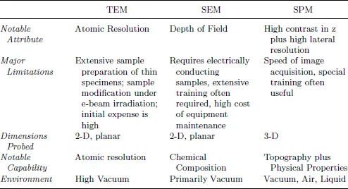
In spite of these successes, the ability to combine compositional identification with electrical and/or mechanical measurements at select locations on a sample surface was a noticeable limitation of the many new surface science tools that were rapidly developed in the 1970s. This clearly identified need, evident in both academic and industrial research labs around the world, might explain the rapid acceptance of SPMs once their basic capabilities were demonstrated. While freely admitting that the attributes and shortcomings of each technique are a matter of personal taste, Table 1.1 attempts to compare TEM, SEM, and SPM.
Finally, it should be remarked that any student working in the world of sub-micron science or engineering requires a good knowledge of many characterization tools to produce credible research results. Knowing which tool to use in what situation can save considerable time in the pursuit of definitive answers to pressing problems. The choice of techniques are large and must include light microscopy, TEM, SEM, SPM, X-ray diffraction (XRD), X-ray Photoemission Spectroscopy (XPS) for elemental analysis, electron spectroscopy (UV photoemission, LEED) for surface analysis, and vibrational spectroscopy (HREELS, FTIR and Raman scattering) for molecular analysis.
Table 1.1 A brief summary of the attributes of different sub-micron microscopies in common use in a modern research laboratory.
1.3 The Scanning Tunneling Microscope
The STM was historically the first SPM and was introduced in 1982 by G. Binnig and H. Rohrer with the demonstration that a controllable vacuum tunnelling gap could be achieved between a sharp metallic tip and a conducting substrate [binnig82]. The vertical resolution of the STM is a few picometers while the lateral resolution can range down to ~0.1nm on an atomically flat substrate. STM i...