![]()
Chapter 1
Introduction
Approaching the end of Moore’s law, we are facing a revolution from traditional microelectronics to a new field called nanoelectronics where all the characteristic lengths are of the order of nanometers. According to the International Technology Roadmap for Semiconductors [1], the device size is expected to shrink continuously from 22 nm (2012) to 14 nm (2014), 10 nm (2016), 7 nm (2018), and 5 nm (2020). The continuous shrinking of the device size results in discontinuous changes in the device physics: At the nanometer scale, electrons behave more like waves than particles, and the well-established semi-classical transport theory needs to be updated to a quantum version; At the nanometer scale, material is no longer continuous, and atomic details may have great impact on the transport properties; At the nanometer scale, the impurities and defects generate considerable randomness, such that disorder effects on the device performance and reliability deserve careful analysis. This chapter aims to provide a physics background and to elaborate some features of nanoelectronic devices.
1.1What is quantum transport?
Before discussing quantum transport, let us first examine the Ohm’s law of classical transport. Ohm’s law says that the current through a resistor is proportional to the applied voltage. At the first glance, the statement is quite natural: Without any voltage, the current must be zero; Applying a small voltage, the current should respond linearly to the driving force. However, there is a loophole in the argument. By definition, the current is proportional to the velocity of electrons, and the voltage is proportional to the electric field or the force exerted on the electrons. According to the Newton’s law, it is the acceleration instead of the velocity that is proportional to the force. Something goes wrong?
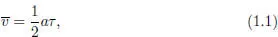
The key to solving the puzzle lies in the fact that Ohmic resistor has a large number of scatterers. In the transport, electrons collide with the scatterers frequently. Imagine an electron has zero velocity at the beginning and is accelerated by the electric field. After flying for a period of time, the electron collides with a scatterer and loses the velocity. After that the electron is accelerated again and collides with another scatterer, and so on and so forth. Therefore the electron moves at an average speed [2]
where a is the acceleration and τ is the average time between two collisions. Eq. (1.1) indicates that the average speed is proportional to the acceleration due to random scattering and hence the puzzle is solved.
The random scattering can be classified into two categories: elastic scattering and inelastic scattering. Elastic scattering means that the electron collides with a “hard” scatterer such that the electron changes its direction but maintains its speed. Inelastic scattering means that the electron collides with a “soft” scatterer such that the electron changes both its direction and speed. In elastic scattering, the energy of the electron is conserved while the momentum is not conserved. In inelastic scattering, both the energy and the momentum of the electron are not conserved. On average an electron may encounter an elastic scatterer after traveling a distance lm or an inelastic scatter after a distance lϕ. The lengths lm and lϕ are referred to as the mean free path and the coherence length respectively. In some cases, lϕ can be much larger than lm. For example, in Si:P δ-doped devices, lϕ is about 80 nm while lm is about 10 nm at 4.2 K [3]. A good discussion of these length scales can be found in Ref. [4].
The coherence length lϕ is a border between the classical world and the quantum world. Notice that the energy E appears in the phase factor e−iEt of a wave function. If the system size is much larger than lϕ, an electron may run into many inelastic collisions which adds a random phase shift to the phase factor. As a result, the phase coherence of the wave function is destroyed and the electron will behave like a particle. If the system size is comparable to or smaller than lϕ, an electron is allowed to conserve its energy and stay in a quantum state described by the wave function ψ(t) = ψ(0) e−iEt. Hence the electron will propagate according to ψ(t) and behave like a wave. In reality, the border between the classical world and the quantum world is not so distinct. The transition from wave-like behavior to particle-like behavior is called dephasing. The two main dephasing mechanisms in semiconductor devices are electron-phonon scattering and disorder scattering. We shall investigate disorder scattering in details in the following chapters.
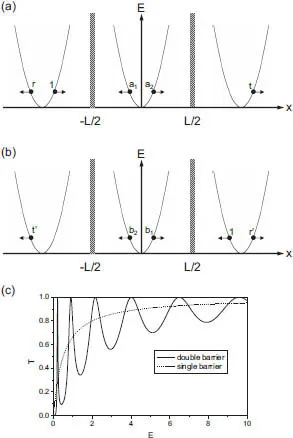
Fig. 1.1 The scattering states and the transmission coefficient of the double δ-barrier model. (a) The incoming wave from the left region is scattered by the double δ-barrier into the reflected wave r and the transmitted wave t. (b) The incoming wave from the right region is scattered by the double δ-barrier into the reflected ...