![]()
Chapter 1
Introduction
Modern society is reliant upon electrical appliances for comfort, transportation, and healthcare. This has motivated great advances in power generation, power distribution and power management technologies based on enhancements in the performance of power devices that regulate the flow of electricity. After the displacement of vacuum tubes by solid state devices in the 1950s, the industry relied upon silicon bipolar devices, such as bipolar power transistors and thyristors. Although the ratings of these devices grew rapidly to serve an ever broader system need, their fundamental limitations in terms of the cumbersome control and protection circuitry led to bulky and costly solutions. The advent of MOS technology for digital electronics enabled the creation of a new class of devices in the 1970s for power switching applications as well. These silicon power MOSFETs have found extensive use in high frequency applications with relatively low operating voltages (under 100 volts). The merger of MOS and bipolar physics enabled creation of yet another class of devices in the 1980s. The most successful innovation in this class of devices has been the Insulated Gate Bipolar Transistor (IGBT)1. The high power density, simple interface, and ruggedness of the IGBT have made it the technology of choice for all medium and high power applications.
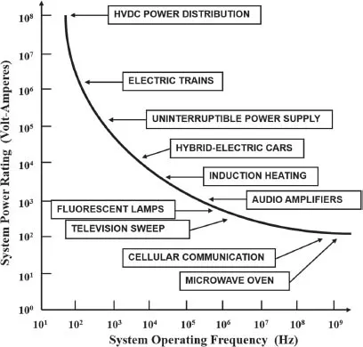
Power devices are required for systems that operate over a broad spectrum of power levels and frequencies. In Fig. 1.1, the applications for power devices are shown as a function of operating frequency. High power systems, such as HVDC power distribution and locomotive drives, requiring the control of megawatts of power operate at relatively low frequencies. As the operating frequency increases, the power ratings decrease for the devices with typical microwave devices handling about 100 watts. All of these applications are served by silicon devices today. Until recently, thyristors were the only devices available with sufficient voltage and current ratings favored for the HVDC power distribution applications. The ratings of IGBTs have now grown to levels where they are now preferred to thyristors for voltage source converters and FACTs designs.
The medium frequency and power applications such as electric trains, hybrid-electric cars, home appliances, compact fluorescent lamps, medical equipment, and industrial motor drives also utilize the IGBT. Power MOSFETs are preferred for the high frequency applications operating from low power source voltages. These applications include power supplies for computers and laptops, power management in smart phones, and automotive electronics.
Fig. 1.1 Applications for power devices.
Another approach for classification of applications for power devices is based on their current and voltage handling requirements as shown in Fig. 1.2. On the high power end of the chart, thyristors are available that can individually handle over 6000 volts and 2000 amperes enabling the control of over 10 megawatts of power by a single monolithic device. These devices are suitable for the HVDC power transmission and locomotive drive (traction) applications. During last 10 years, IGBT modules have been developed with blocking voltages of up to 6500 volts and current handling capability above 1000 amperes. This has allowed the IGBT to replace thyristors in HVDC and traction applications.
For the broad range of systems that require operating voltages between 300 volts and 3000 volts with significant current handling capability, the IGBT was found to be the optimum solution since the 1990s. These applications span all sectors of the economy including consumer, industrial, transportation, lighting, medical, defense, and renewable energy generation1.
When the current requirements fall below 1 ampere, it is feasible to integrate multiple devices on a single monolithic chip to provide greater functionality for systems such as telecommunications and display drives. However, when the current exceeds a few amperes, it is more cost effective to use discrete power MOSFETs with appropriate control ICs to serve applications such as automotive electronics and switch mode power supplies.
Fig. 1.2 System ratings for power devices.
1.1 Ideal and Typical Power Device Characteristics
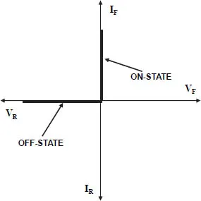
An ideal power rectifier should exhibit the i-v characteristics shown in Fig. 1.3. In the forward conduction mode, the first quadrant of operation the figure, it should be able to carry any amount of current with zero on-state voltage drop. In the reverse blocking mode, the third quadrant of operation in the figure, it should be able to hold off any value of voltage with zero leakage current. Further, the ideal rectifier should be able to instantaneously switch between the on-state and the off-state with zero switching time. The ideal power rectifier would then dissipate no power while allowing control of the direction of current flow in circuits.
Fig. 1.3 Characteristics of an ideal power rectifier.
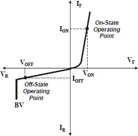
Actual power rectifiers exhibit the i-v characteristics illustrated in Fig. 1.4. They have a finite voltage drop (VON) when carrying current (ION) on the on-state leading to ‘conduction’ power loss. The doping concentration and thickness of the drift region of the power device must be carefully chosen based upon the desired breakdown voltage2. Smaller drift region doping levels with larger thickness are needed to support larger voltages. This increases the on-state voltage drop in rectifiers with increasing blocking voltage ratings. They also have a finite leakage current (IOFF) when blocking voltage (VOFF) in the off-state producing power loss. In addition, power rectifiers switch from the on-state to the off-state in a finite time interval and display a large reverse recovery current before settling down to the off-state operating point. The reverse recovery process can produce power losses as great as those observed in the on-state.
Fig. 1.4 Characteristics of a typical power rectifier.
The finite power dissipation in the power rectifier produces internal heating. This limits the maximum on-state current density to maintain an acceptable maximum junction temperature. The power dissipated in a power rectifier is given by:
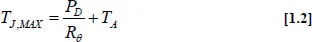
where the first term is the on-state power loss, the second term is the off-state power loss, and the third term is the switching power loss. The on-state current density (JON) is determined by the maximum junction temperature (TJ,MAX):
where Rθ is the thermal impedance and TA is the ambient temperature. The power dissipation in power devices increases when their voltage rating is increased due to an increase in the on-state voltage drop and switching loss per cycle. The typical on-state current density for power devices ranges from 25 to 150 A/cm2 depending up on the blocking voltage rating and the packaging technology.
The i-v characteristics of an ideal power switch designed for operation from a DC power source are illustrated in Fig. 1.5. As in the case of the ideal rectifier, the ideal transistor conducts current in the on-state with zero voltage drop and blocks voltage in the off-state with zero leakage current. In addition, the ideal device can operate with a high current and voltage in the active region with the forward current in this mode controlled by the applied gate bias. The spacing between the characteristics in the active region is uniform for an ideal transistor indicating a gain that is independent of the forward current and voltage.
Fig. 1.5 Characteristics of an ideal transistor.
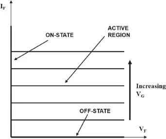
The i-v characteristics of a typical power switch are illustrated in Fig. 1.6. This device exhibits a finite resistance when carrying current in the on-state as well as a finite leakage current while operating in the off-state (not observable in the figure because its value is much lower than the on-state current levels). The breakdown voltage of a typical transistor is also finite as indicated in the figure with ‘BV’ where the current abruptly increases. The typical transistor can operate with a high current and voltage in the active region. This current is controlled by the base current for a bipolar transistor while it is determined by a gate voltage for a MOSFET or IGBT (as indicated in the figure). It is preferable to have gate voltage controlled charact...