![]()
INTRODUCTION
The global power semiconductor market size, according to the published forecasting data by manufacturers, is likely to attain 30 billion US dollars in the year 2020. Within this segment, for those using next-generation wide bandgap materials such as SiC and GaN, the global market may reach 3 billion US dollars in 2020. The slow growth of the wide bandgap devices is mainly due to issues of cost and reliability. However, the situation is expected to improve.
From the application point of view, in analogy to a human body, the microprocessors or digital signal processors perform “thinking” and calculations to make desirable decisions in electronic systems somehow similar to what the human brain does. Once a decision is made, it frequently needs to be put in work by the peripheral power train, just like human arms and legs. The power train provides high voltage, high current static energy conversion or dynamic motion control involving mechanical actuation to interact with the real world. Power semiconductor devices are the building elements for the power train. They are used to handle the high voltage and high current loads at high temperature.
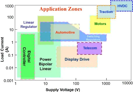
The boundary to differentiate a power semiconductor device from the semiconductor device group sometimes can be unclear as it can be made from the same CMOS compatible process as well as be seamlessly integrated with other low power semiconductor components. In general, we can look at the main functionality of the device and its power rating in order to identify it to be a power semiconductor device. As indicated in Fig. 1.1, the application of such a device ranges from the linear regulator of a few hundred milliwatts to traction and HVDC of a few hundred megawatts. Clearly, the range of applications is very wide, and these devices vary from low-power CMOS microchips at one end to Megawatt wafer-level large vertical configuration at the other end. Three basic specifications are looked at to determine whether a power device is suitable for a particular application, namely, the voltage rating, the current rating, and the switching frequency (or the switching speed). Or, if the device is to be used for linear application, i.e. non-switching, instead of the switching speed, the small signal gain, the bandwidth, and the power rating will also be looked at.
Fig. 1.1. The various application zones of power semiconductor devices in terms of system voltage and load current.
The desirable features of a power semiconductor device for switching application are to have a high voltage sustaining ability with very low leakage current; a high current rating with very low on-state resistance; a fast switching speed with minimum losses; high noise immunity and to be latch-up free. Similarly, for the linear application, it is to have a high small signal gain with low harmonic distortion; a wide bandwidth and good power rating. In order to achieve all of these, research in several areas, namely, the material, the fabrication processes, the device structures, integration, and packaging were looked into. For the material, although silicon is still the mainstream material for power semiconductor devices, wider bandgap materials such as silicon carbine, gallium nitride, carbon, or strained silicon germanium are getting widely accepted to make devices with better performance. However, the limitation sits on the availability of good quality source wafers and the high-yield fabrication processes. For the fabrication processes, special recipes were constantly developed to meet the requirement of advanced structures. Modern power semiconductor devices can now be categorized into several mature types, namely, the diode, the BJT, the thyristor (and GTO), the MOSFET, the IGBT, and the static induction transistor. These devices, except for MOSFET, are bipolar in nature and suitable for high current conduction. MOSFET, on the other hand, has good switching performance and simple gate drive requirement for medium-power products. Isolation and integration technology for devices of lateral structure are also an important focus for power integrated circuits. Overall, the research and development work is closely linked to fabrication processes which can be rather costly. Industrial companies play an important role in the development of new devices and processes.
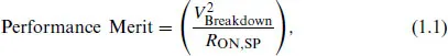
Among all power semiconductor devices, MOSFETs and IGBTs are playing major roles in applications and will continue to be the devices in high demand for medium–high voltage applications. The silicon superjunction technology for MOSFET has increased the device voltage rating and reduced its specific on-state resistance, thus making the device to break the unipolar silicon limit. Recently, wide bandgap devices became a popular trend in power semiconductor devices both in research and development, and in industrial commercialization. These involve the growth of suitable substrates, epitaxy buffer layers, new process recipes, and new dielectric materials and device structures. The performance merit of a power device can be rated by the following relationship:
where VBreakdown is the device breakdown voltage in volts and RON,SP is the on-state specific resistance in Ω · cm2. Typically, for silicon power MOSFET, the performance merit is around 30–50 × 106 V2/(Ω · cm2). For gallium nitride MISHEMT, it is around 300–500 × 106 V2/(Ω · cm2). And, for SiC MOSFET, it can be as high as 800–1000 × 106 V2/(Ω · cm2). Wide bandgap devices are expected to have a sizeable market share.
SiC has always been one of the material candidates for semiconductor devices since the invention of diodes and transistors. However, with the rapid advancement of Si technology, it was ignored most of the time, until the breakthroughs in crystal growth and epitaxy of SiC in 1980s. The availability of electronic grade material greatly facilitates the development of SiC devices for power electronic applications. Today, six-inch SiC wafers with more than 50 μm and less than 1 × 1015 cm−3 doped epi-layers are commercially available, serving as the fundamental building block of modern SiC devices. After their introduction into the power device market by Infineon and Cree in 2001, SiC Schottky diodes have demonstrated their capability to significantly improve the system efficiency and power density, and have been widely adopted in some applications. It is fair to say that they have established their reputation and the market share will only grow in the foreseeable future. On the other hand, SiC switches are still facing challenges from the prevailing Si devices, mainly because of the cost issues and unproven reliability. Consensus is that SiC switches will most likely penetrate the market in the high-end and high-voltage sector first where cost is less of an issue. With the help of recent advancements in defect and carrier lifetime control, SiC bipolar devices have started to show excellent performance with much improved reliability for possible ultra-highvoltage applications. Despite the bright future of SiC devices, material costs and peripherals such as packaging and circuitry are the current bottlenecks which will eventually determine the speed and extent of SiC device’s success. Nevertheless, the presence of SiC devices pushes the envelope of power electronics limits to higher frequency and power density.
Unlike SiC power devices, the AlGaN/GaN heterojunction induces two-dimensional (2D) electronic polarization charges which form a natural conduction channel. Such a conduction channel makes the AlGaN/GaN device a default normally-on device. The immediate application will be for the RF power amplifier where the operating point is at the normally-on state for large signal swing. Recently, normally-off structures were developed for power electronic applications. To enable normally-off operations, the gate structure is modified from the simple Schottky gate to a p-GaN gate or full trenched gate or fluorinated gate. The trade-off in making normally-off gate is on getting a high positive threshold voltage (above 3.5 V) and a good high temperature threshold stability. Besides, the current collapse phenomenon is another important concern in power electronic application. Multiple field plates and better surface passivation are used to reduce the current collapse. Another option is the usage of two-dimensional hole gas (2DHG) on the top layer to reduce the surface field (RESURF) between the gate and drain in lateral direction, allowing higher voltages to be applied.
The advent of SiC and GaN devices has added newer processing techniques in power device technology. SiC or p-type GaN dopant activation requires higher temperature processing compared to that in silicon technology. Atomic layer deposition (ALD) method and plasma treatment for the introduction of desired impurities have been extensively used in CMOS technology but they are rarely needed in power devices as the junctions are typically deep and dielectric thickness is large compared to what CMOS needs. However, the use of thin dielectric to reduce the gate leakage and low energy F plasma treatment to introduce F with shallow depth to raise threshold voltage has been adapted for GaN devices. Hence, these advanced processing techniques have become part of GaN-based power MISHEMT device processing. Case studies that use these methods are included in this edition.
This book aims to introduce power semiconductor devices and fabrication technology to readers who are interested or involved in this important field of technology. Chapter 2 provides fundamentals for junction electrostatics and breakdown analyses. Chapter 3 focuses on p–n junction rectification aspects. Chapters 4 and 5 are on devices of MOSFET and IGBT. Chapter 6 discusses the new superjunction structure which breaks the unipolar silicon limit in performance merit. Chapter 7 looks into the wide bandgap SiC power devices and Chapter 8 is on the AlGaN/GaN heterojunction polarization and HEMT devices. Chapters 9–11 look into the fabrication process technology and case studies including both the superjunction and wide bandgap devices. Overall, the book is a good reference material for both detailed theory and technology work in the field of power semiconductor devices.
![]()
CARRIER PHYSICS AND JUNCTION ELECTROSTATICS
2.1.Introduction
To understand the operating characteristics of power semiconductor devices well it requires a good background knowledge in semiconductor physics, in particular on carrier transport and junction electrostatics. For this chapter, some important concepts on carrier transport physics and junction electrostatics with breakdown mechanisms of silicon (Si) semiconductor are reviewed. Materials of gallium arsenide (GaAs) and silicon carbide (SiC) are also briefly mentioned. The aim of this chapter is not to treat the semiconductor physics rigorously in fundamental detail. Rather, it is to highlight those properties that are important and needed in understanding the operational characteristics of power semiconductor devices.
2.2.Crystal Structure and Energy Bands
Silicon belongs to the group IV element and as such it has four valence electrons in its outermost shell. Silicon crystallizes in a diamond structure in which four atoms are located at the corners of opposite diagonals of the cube and they surround one atom in the center of the cube, as shown in Fig. 2.1. The central atom has four covalent shared-pair electron bonds with the surrounding four atoms. The unit cell lattice constant a is 5.43 Å. It has eight corner atoms, six face atoms, and four central atoms for a total of eight atoms in the unit cell. Since there are eight silicon atoms per unit cell and the volume of the unit cell is a3, it follows that there are 5 × 10²² atoms/cm3 in the silicon lattice. It is this structu...