![]()
PART 1
MOSFET Fundamentals
![]()
Lecture 1
Overview
1.1 Introduction
1.2 Electronic devices: A very brief history
1.3 Physics of the transistor
1.4 About these lectures
1.5 Summary
1.6 References
1.1Introduction
The transistor has been called “the most important invention of the 20th century” [1]. Transistors are everywhere; they are the basic building blocks of electronic systems. As transistor technology advanced, their dimensions were reduced from the micrometer (μm) to the nanometer (nm) scale, so that more and more of them could be included in electronic systems. Today, billions of transistors are in our smartphones, tablet and personal computers, supercomputers, and the other electronic systems that have shaped the world we live in. In addition to their economic importance, transistors are scientifically interesting nano-devices. These lectures aim to present a clear treatment of the essential physics of the nanotransistor. This first lecture introduces the topics we’ll discuss and gives a roadmap for the remaining lectures.
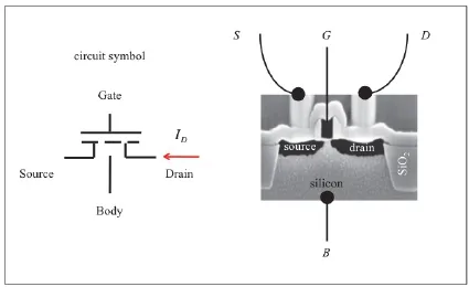
Figure 1.1 shows the most common transistor in use today, the Metal-Oxide-Semiconductor Field-Effect Transistor (MOSFET). On the left is the schematic symbol we use when drawing transistors in a circuit, and on the right is a scanning electron micrograph (SEM) of a silicon MOSFET circa 2000. The transistor consists of a source by which electrons enter the device, a gate, which controls the flow of electrons from the source and across the channel, and a drain through which electrons leave the device. The gate insulator, which separates the gate electrode from the channel, is less than 2 nm thick (less than the diameter of a DNA double helix). The length of the channel was about 100 nm at the turn of the century, and is about 20 nm today. The operation of a nanoscale transistor is interesting scientifically, and the technological importance of transistors is almost impossible to overstate.
Fig. 1.1 The silicon MOSFET. Left: The circuit schematic of an enhancement mode MOSFET showing the source, drain, gate, and body contacts. The dashed line represents the conductive channel, which is present when a large enough gate voltage is applied. Right: An SEM cross-section of a silicon MOSFET circa 2000. The source, drain, gate, silicon body, and gate insulator are all visible. The channel is the gap between the source and the drain. (Source: Texas Instruments, circa 2000.)
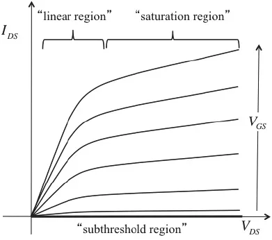
Figure 1.2 shows the current-voltage (IV) characteristics of a MOSFET. Electrons flow from the source to the drain when the gate voltage is large enough. Devices with IV characteristics like this are useful in electronic circuits. They can operate as digital switches, either on or off, or as analog amplifiers of input signals. The shape of the IV characteristic and the magnitude of the current are controlled by the physics of the device. My goal in these lectures is to relate the IV characteristic of a nanotransistor to its internal physics.
Fig. 1.2 The common source output IV characteristics of an N-channel MOSFET. The vertical axis is the current that flows between the drain and source terminals, and the horizontal axis is the voltage between the drain and source. Each line corresponds to a different gate voltage. The two regions of operation, to be discussed later, are also labeled. The maximum voltage applied to the gate and drain terminals is the power supply voltage, VDD. (The small leakage current in the subthreshold region is not visible on a linear scale for IDS.)
1.2Electronic devices: A very brief history
Electronic systems are circuits of interconnected electronic devices. Resistors, capacitors and inductors are very simple devices, but most electronic systems rely on non-linear devices, the simplest being the diode, which allows conduction for one polarity of applied voltage but not for the other. The first use of diodes was for detecting radio signals. In the early 1900’s, semiconductor diodes were demonstrated as were vacuum tube diodes. Semiconductor diodes were metal-semiconductor junctions consisting of a metal wire (the “cat’s whisker”) placed in a location on the crystal that gave the best performance. Because they were finicky, these crystal detectors were soon replaced with vacuum tube detectors, which consisted of a heated filament that boiled off electrons and a metal plate inside an evacuated bulb. When the voltage on the plate was positive, electrons from the filament were attracted, and current flowed.
The vacuum tube triode quickly followed the vacuum tube diode (and, later, the pentode). By placing a metal grid between the filament and plate, a large current could be controlled with a small voltage on the grid, and signals could be amplified. The widespread application of vacuum tubes transformed communications and entertainment and enabled the first digital computers, but vacuum tubes had problems — they were large, fragile, and consumed a lot of power.
In the 1920’s, Julius Lilienfeld and Oskar Heil independently patented a concept for a “solid-state” replacement for the vacuum tube triode. By eliminating the need for a heated filament and a vacuum enclosure, a solid-state device would be smaller, more reliable, and consume less power. Semiconductor technology was too immature at the time to develop this concept into a device that could compete with vacuum tubes, but by the end of World War II, enough ground work had been laid to spur Bell Telephone Laboratories to mount a serious effort to develop a solid-state replacement for the vacuum tube [2]. The result, in December 1947, was the transistor – not the field-effect transistor (FET) of Lillenfeld and Heil but a point contact bipolar transistor (something like the original cat’s whisker crystal rectifier). Over the years, however, the technological problems associated with FETs were solved, and today, the Metal-Oxide-Semiconductor Field-Effect Transistor (MOSFET) is the mainstay of electronic systems [3]. These lectures are about the MOSFET, but the basic principles apply to several different types of transistors.
By 1960, technologists learned how to...