![]()
Chapter 1
Digital Signal Processing for Optical Coherent Long-Haul Transmission System
1.1.Introduction
Coherent optical communication based on digital signal processing (DSP) for long-haul transmission system has been proved to be a great success in the last decade [1–20]. However, coherent optical communication itself is not a new technology, people have started the research over 40 years ago, and the first coherent detection experimental demonstration was reported in 1970s [1–5]. The early stage of research is not accepted by the industry due to the complexity of phase, frequency and polarization tracking. After a long-time stagnation during the time of intensity modulation and direct detection (IM/DD), digital coherent optical communication based on DSP has again revolutionized the optical communication for high-speed, high-capacity and long-distance transmission [21–37].
With the development and maturation of high-speed digital-to-analog convertor (DAC), analog-to-digital converter (ADC) and application-specific integrated circuit (ASIC), DSP for high-speed optical signal becomes possible, which moves the complexity of phase, frequency and polarization tracking into the digital domain [9–20]. Therefore, it simplifies the reception of advanced modulation formats (i.e., quadrature phase shift keying (QPSK), 16QAM, 64QAM) and also enables the major electrical and optical impairments (bandwidth limitation, chromatic dispersion, polarization mode dispersion, fiber nonlinear impairments) being processed and compensation in the digital domain at the transmitter or receiver side. Therefore, the DSP-based coherent optical communication system has become an active research topic, which is a promising technology for future high spectrum efficiency and high-speed transmission.
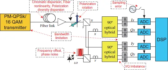
Fig. 1.1.The typical digital coherent system and the impairments from the system, which are needed to be handled using the advanced DSP.
The chapter will introduce the recent progress of DSP for high-speed and long-haul optical coherent transmission system. Figure 1.1 shows the typical digital coherent system and the impairments from the system, which are needed to be handled using the advanced DSP. Section 1.2 will introduce the classic DSP algorithms used in the coherent system, then Section 1.3 will discuss the digital pre-equalization for bandwidth limited system. Advanced DSP for fiber nonlinearity compensation is introduced in Section 1.4. Finally, Section 1.5 summarizes this chapter.
1.2.DSP for Digital Coherent System at Receiver Side
1.2.1.The basic DSP blocks
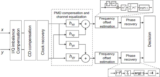
The typical digital coherent receiver with DSP for signal equalization and recovery are shown in Fig. 1.2 [2, 3]. The optical signal is coherently detected by a polarization and phase diverse hybrid with a local oscillator, which converts the optical signals into electrical signals with both in-phase and quadrature (I/Q) signals in X and Y polarizations after balanced photodetectors. The electrical signals after PDs are then sampled and digitized by the ADCs and then are processed by the DSP as shown in Fig. 1.2. Generally, the DSP at the receiver side can be divided into several subsystems or subunits, and each of them is applied to handle one specific impairment in the transmission link and transponders.
Fig. 1.2.Basic DSP blocks at the receiver side for coherent optical communication [2, 3].
Ideally, the I and Q signals should be orthogonal to each other. However, in the practical system, the I/Q signals are not orthogonal to each other due to the imbalance between these two components. These imbalances can be caused by bias drift, device defect of modulators and PDs or power differences after drivers. In order to get the signals recovered correctly, I/Q imbalance compensation should be applied first to the digitized signals. This process can be carried out by using the Gram–Schmidt Orthogonalization Process (GSOP) algorithm [4]. The GSOP creates a set of mutually orthogonal vectors, taking the first vector as a reference against which all subsequent vectors are orthogonalized [2]. The GSOP algorithm is an effective method for converting the unbalanced or non-orthogonal data samples to the balanced and orthogonal data samples.
1.2.2.Chromatic dispersion linear channel equalization
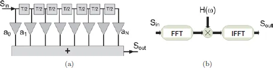
After that, the signals are then processed by the linear signal process to electrically compensate the chromatic dispersion (CD). The channel response of a fiber with CD can be represented as a linear function. CD compensation can be realized at the receiver side in frequency domain or time domain (Fig. 1.3) [2, 3].
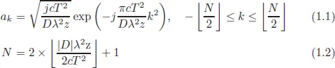
The digital CD compensation can be processed in either time domain based on finite impulse response (FIR) or frequency domain based on the transfer function. In time domain, the required filter coefficients for FIR can be obtained by the fiber CD transfer function using either the frequency-domain truncation method or the time-domain truncation method [3]. The FIR coefficient of each tap ak can be calculated by the following equations:
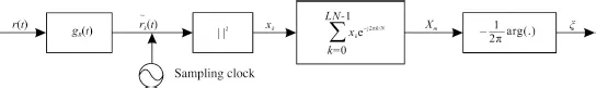
Fig. 1.3.(a) Time-domain FIR structure of CD compensation and (b) frequency-domain CD compensation based on the FFT and IFFT processes.
In the above equations, D is the dispersion coefficient, λ is the wavelength and z is the fiber length, c is the speed of light, T is the symbol period, k is the order of taps, and N is the total number of FIR taps.
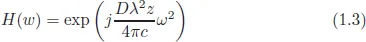
For short distance, time-domain method shows less complexity, however, for long-haul transmission (over 1000km), frequency-domain equalization (FDE) based on FFT shows less computation complexity:
The frequency-domain channel response is shown in Eq. (1.3). When doing the frequency-domain CD compensation, one needs to transfer the data into frequency domain by using the FFT process. After multiplying the transfer function, the data can be recovered by the IFFT process.
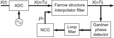
1.2.3.Clock recovery
The other impairments, such as the timing offset caused by the ADC can also be compensated in the digital domain, known as the clock-recovery algorithms [5–7]. Several classical timing phase estimation and recovery schemes can be successfully applied in the coherent optical communication system, such as the square-timing recovery [5], Gardner-timing recovery [6] and Godard scheme [7].
Fig. 1.4.Square-timing recovery based on feedforward structure.
Fig. 1.5.Gardner-timing recovery method based on feedback loop with error update.
Generally, the square-timing recovery is a feedforward method as shown in Fig. 1.4, and it requires at least four samples per symbol to find the right clock information. Therefore, it cannot track the clock offset and has large computation complexity.
Another method, Gardner-timing recovery widely used in the digital coherent system, only requires two samples per symbol. On the other hand, it is feedback-type algorithm (Fig. 1.5).
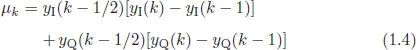
Assume the kth symbol with the I and Q components as {yI(k)}, {yQ(k)} and {yI(k − 1/2)}, {yQ(k − 1/2)}. Then, according to the Gardner time recovery algorithm [6], the error function for the clock update is based on the following equation:
1.2.4.Polarization demultiplexing and PMD compensation
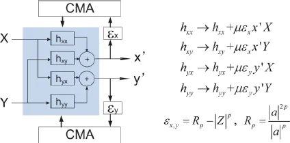
As analyzed above, there are two linear impairments that would affect the polarization multiplexed (PM) signals. To obtain the data for each polarization, one needs to do polarization demultiplexing and polarization mode dispersion (PMD) compensation. After that, the following four adaptive butterfly equalizers are used for polarization demultiplexing, channel equalization and also PMD compensation.
Fig. 1.6.The four adaptive butterfly equalizers based on CMA and its updating functions.
Figure 1.6 shows the structure and the principle of signal recovery by the adaptive and butterfly equalizers based on constant modulus algorithm (CMA) and also the filter coefficients updating equations. The cost function and error function are based on the modules of the output and input data. The linear distortions caused by optical filtering effects in the link are also equalized by the time-domain FIR filters. Generally, T/2-spaced FIR filters are used in the DSP and the filter coefficients are adaptively u...