![]()
CHAPTER 1
LATCH AND FLIP FLOP CIRCUITS
1.1. INTRODUCTION
In Volume II Chapter 3 we discussed combinational logic circuits whose outputs depended upon their inputs. These inputs and outputs cannot retain their logic levels for future storage capability further operations. Unlike combinational logic circuits, several digital system circuits have the ability to store data, which requires memory capacity. These circuits are referred to as sequential logic circuits and depend on their previous and current state inputs. Their outputs will be tied back to their inputs in some respect, providing the necessary feedback of their circuits. Latch and flip flop circuits are these types of digital circuits. The latch circuit forms the basic core for the foundation of flip flops. In this chapter we will learn about the different types of latch and flip flop circuits.
Additionally, it is critical to understand that Transistor-Transistor Logic (TTL) and Complementary Medal-Oxide Semiconductor (CMOS) devices have special characteristics to prevent design flaws and damage to chips. Many of the electrical behaviors with discrete circuits also apply to these materials. These special characteristics will also be discussed in this chapter.
1.2. ACTIVE LOW LATCH—NAND GATE LATCH
The active low latch has two inputs, identified as SET′ and CLR′, hence active low latch. The latch outputs are Q and Q′. Figure 1.1 shows how one NAND gate output feeds back to the other NAND gate input with opposite polarity, the state of each input combination, the logic symbol for the active low latch, and the active low latch waveform.
Figure 1.1. Active low latch logic diagrams and state table
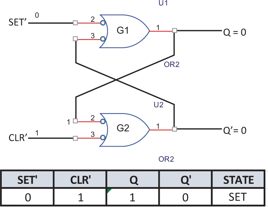
Gate latch SET′ and CLR′ level will be explained next. As shown in Figures 1.2 to 1.5, the completed aforementioned active low latch state table is analyzed. We began with SET′ = 0 and CLR′ = 1, as shown in Figure 1.2, where the output of logic gate G1 is a logic high or 1. This logic 1 is feedback from the output of gate G1 to the top input of logic gate G2. This input logic 1 along with the CLR′ logic 1 will produce a logic low or logic 0 output to logic gate G2. When the SET′ = 0 and CLR′ = 1 inputs exist, this condition places the active low latch in a SET state as shown in the state table in Figure 1.2.
Figure 1.2. SET state of the active low latch
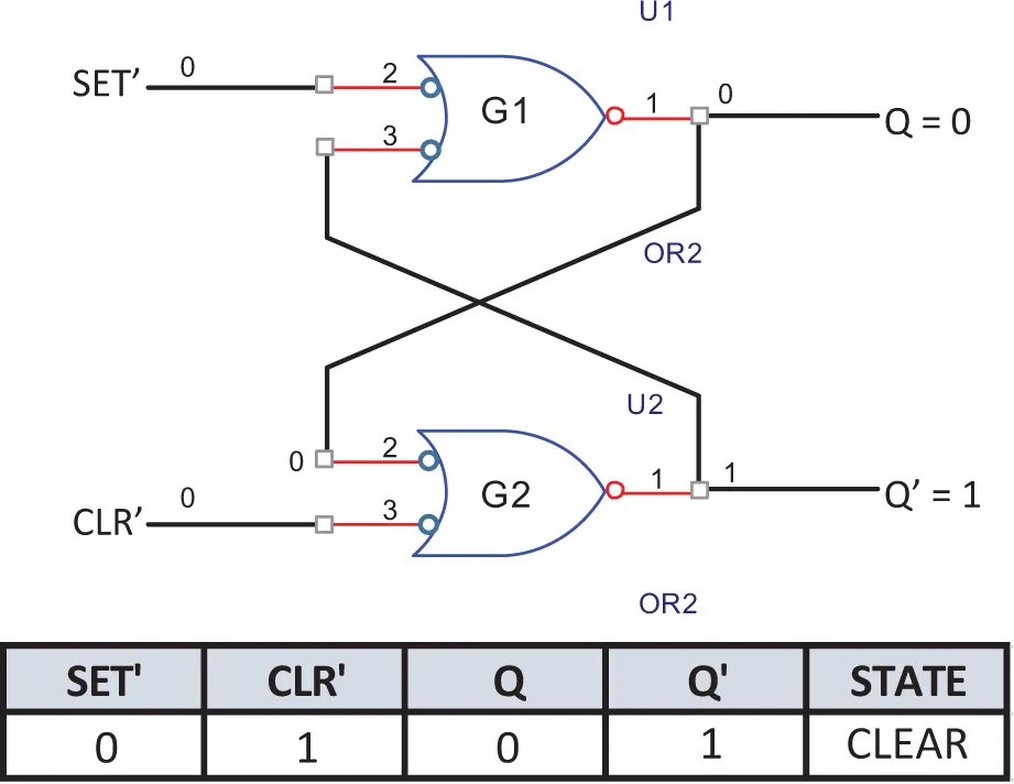
Next we show SET′ = 1 and CLR′ = 0 in Figure 1.3, where the output of logic gate G1 is a logic low or logic 0. This logic 0 is feedback from the output of gate G1 to the top input of logic gate G2. This input logic 0 along with the CLR′ logic 0 will produce a logic high or logic 1 output to logic gate G2. When the SET′ = 1 and CLR′ = 0 inputs exist, this condition places the active low latch in a CLEAR state as shown in the state table in Figure 1.3.
Figure 1.3. CLEAR state of the active low latch
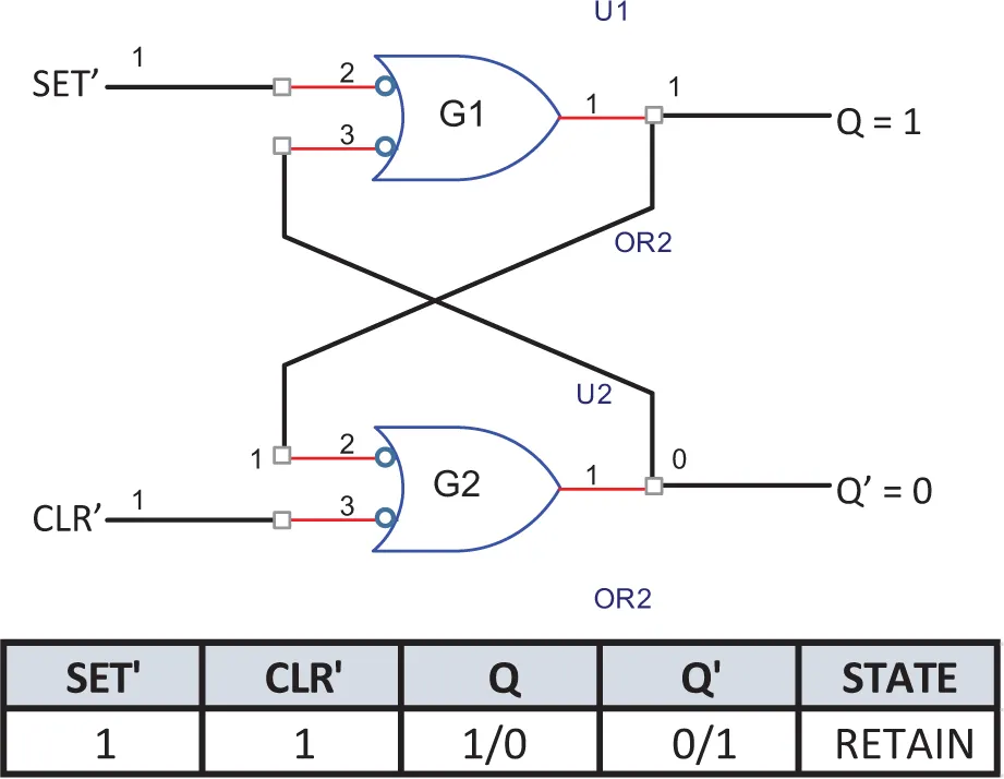
Next we show SET′ = 1 and CLR′ = 1. In Figure 1.4, we assume that the latch circuit is in the SET state where Q = 1 and Q′ = 0. We can assume that the circuit is either in the SET or the CLEAR state. In order to explain our current input condition of SET′ = CLEAR = 1, we simple trace back from the Q′= 0 output to the lower input to gate G1. The low input causes gate G1′s output to retain a logic 1 output. When tracking back from the logic 1 G1 output to the upper G2 input we have two logic 1 inputs causing the Q′ output of a logic 0. When both circuit inputs are high or logic 1 the latch will retain the state it was in previously. We can analyze both SET and CLEAR states of the latch circuit and determine that the latch will be in the RETAINed state. Figure 1.4 shows the RETAIN state of the previous latch state—the previous SET state in our example.
Figure 1.4. RETAIN state of the a...