Molecular Beam Epitaxy
eBook - ePub

Molecular Beam Epitaxy

Materials and Applications for Electronics and Optoelectronics

  1. English
  2. ePUB (mobile friendly)
  3. Available on iOS & Android
eBook - ePub

Molecular Beam Epitaxy

Materials and Applications for Electronics and Optoelectronics

About this book

Covers both the fundamentals and the state-of-the-art technology used for MBE

Written by expert researchers working on the frontlines of the field, this book covers fundamentals of Molecular Beam Epitaxy (MBE) technology and science, as well as state-of-the-art MBE technology for electronic and optoelectronic device applications. MBE applications to magnetic semiconductor materials are also included for future magnetic and spintronic device applications.

Molecular Beam Epitaxy: Materials and Applications for Electronics and Optoelectronics is presented in five parts: Fundamentals of MBE; MBE technology for electronic devices application; MBE for optoelectronic devices; Magnetic semiconductors and spintronics devices; and Challenge of MBE to new materials and new researches. The book offers chapters covering the history of MBE; principles of MBE and fundamental mechanism of MBE growth; migration enhanced epitaxy and its application; quantum dot formation and selective area growth by MBE; MBE of III-nitride semiconductors for electronic devices; MBE for Tunnel-FETs; applications of III-V semiconductor quantum dots in optoelectronic devices; MBE of III-V and III-nitride heterostructures for optoelectronic devices with emission wavelengths from THz to ultraviolet; MBE of III-V semiconductors for mid-infrared photodetectors and solar cells; dilute magnetic semiconductor materials and ferromagnet/semiconductor heterostructures and their application to spintronic devices; applications of bismuth-containing III–V semiconductors in devices; MBE growth and device applications of Ga2O3; Heterovalent semiconductor structures and their device applications; and more.

  • Includes chapters on the fundamentals of MBE
  • Covers new challenging researches in MBE and new technologiesĀ 
  • Edited by two pioneers in the field of MBE with contributions from well-known MBE authors including three Al Cho MBE Award winners
  • Part of the Materials for Electronic and Optoelectronic Applications series

Molecular Beam Epitaxy: Materials and Applications for Electronics and Optoelectronics will appeal to graduate students, researchers in academia and industry, and others interested in the area of epitaxial growth.

Frequently asked questions

Yes, you can cancel anytime from the Subscription tab in your account settings on the Perlego website. Your subscription will stay active until the end of your current billing period. Learn how to cancel your subscription.
At the moment all of our mobile-responsive ePub books are available to download via the app. Most of our PDFs are also available to download and we're working on making the final remaining ones downloadable now. Learn more here.
Perlego offers two plans: Essential and Complete
  • Essential is ideal for learners and professionals who enjoy exploring a wide range of subjects. Access the Essential Library with 800,000+ trusted titles and best-sellers across business, personal growth, and the humanities. Includes unlimited reading time and Standard Read Aloud voice.
  • Complete: Perfect for advanced learners and researchers needing full, unrestricted access. Unlock 1.4M+ books across hundreds of subjects, including academic and specialized titles. The Complete Plan also includes advanced features like Premium Read Aloud and Research Assistant.
Both plans are available with monthly, semester, or annual billing cycles.
We are an online textbook subscription service, where you can get access to an entire online library for less than the price of a single book per month. With over 1 million books across 1000+ topics, we’ve got you covered! Learn more here.
Look out for the read-aloud symbol on your next book to see if you can listen to it. The read-aloud tool reads text aloud for you, highlighting the text as it is being read. You can pause it, speed it up and slow it down. Learn more here.
Yes! You can use the Perlego app on both iOS or Android devices to read anytime, anywhere — even offline. Perfect for commutes or when you’re on the go.
Please note we cannot support devices running on iOS 13 and Android 7 or earlier. Learn more about using the app.
Yes, you can access Molecular Beam Epitaxy by Hajime Asahi, Yoshiji Horikoshi, Hajime Asahi,Yoshiji Horikoshi in PDF and/or ePUB format, as well as other popular books in Physical Sciences & Optics & Light. We have over one million books available in our catalogue for you to explore.

Information

Publisher
Wiley
Year
2019
Print ISBN
9781119355014
eBook ISBN
9781119355021

Part I
Fundamentals of MBE

1
History of MBE

Tom Foxon
Department of Physics and Astronomy, Nottingham University, Nottingham, NG7 2RD, UK

1.1 Introduction

John Orton and I have recently published a book entitled Molecular Beam Epitaxy – A Short History [1]. In that book we were not able to cover all aspects of this topic, so many significant contributions had to be omitted. In this short chapter, even more work of importance will be missing and what follows is my personal view of how molecular beam epitaxy (MBE) evolved. Before starting to describe how it occurred, we have of course to decide what we mean by MBE. As far as I can discover, the term was first used in the Proceedings of the Third International Symposium on GaAs and Related Compounds by Cho et al. [2] in order to distinguish MBE from the earlier growth methods, namely liquid phase epitaxy (LPE) and vapour phase epitaxy (VPE). So, what is MBE? One may consider it to be a refined form of vacuum evaporation, but it is clearly significantly different from simple evaporation in many ways. It usually involves multiple sources and deposition onto a heated substrate. It usually takes place in ultra‐high vacuum (UHV) equipment, in order to reduce the arrival rate of unwanted species. In general, collision‐free molecular beams are used to supply the required species to the substrate. It differs from many other growth methods in having many different in‐situ measurements (e.g. electron diffraction or mass spectrometry), which enables the process to be controlled at an atomic level. My personal view is that there are at least two MBE topics of equal importance, there is the study of the MBE process itself and the application of MBE to provide samples and devices of the highest possible quality. In my career I have been involved in both aspects for a variety of material systems and regard them as equally significant. In this chapter I will try to summarise what went into our book and will begin by discussing the development of the MBE process before turning to its application. Before starting on this task, I recommend to the reader two review articles published by three of the pioneers of MBE in 1974 [3] and 1975 [4], respectively. The first deals with epitaxy in general, whilst the second deals exclusively with MBE and gives a comprehensive account of the state of the art at that time (1975).
In what follows I will try to avoid too much overlap with the following chapters, so comments on devices, magnetic semiconductors and new materials will be very brief.

1.2 The MBE Process

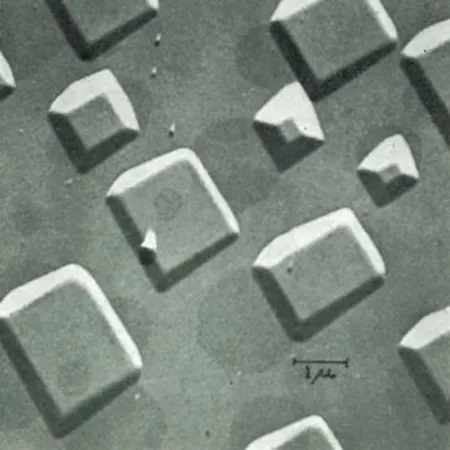
As far as I am aware, the first studies of growth, by what we now call MBE, were performed at Plessey Labs in Caswell by Bruce Joyce and co‐workers. They grew Si films from molecular beams of silane on a heated Si substrate under UHV conditions and the resulting samples were studied by Roger Booker at Cambridge University using transmission electron microscopy (TEM). This study was concerned with the nucleation process itself and very low growth rates were used in order to separate reactions on the surface from those in the gas phase, hence the need for collision‐free molecular beams. This work was published in a series of papers from 1966 onwards [5–7] and was summarised in a review article by Bruce Joyce in 1968 [8]. The equipment used for this study had many of the attributes of a modern MBE system (having collimated, collision‐free, molecular beams of silane impinging on a heated Si substrate) and took place under UHV conditions; the pressure during growth in the reaction chamber was ∼3 Ɨ 10āˆ’9 Torr. The growth rates were small compared to modern practise and no in‐situ characterisation was involved, but in all other respects this could be considered to be the first study of the MBE growth process. A result from this study is shown in Figure 1.1, where it is clear that Si grows epitaxially on the heated Si substrate by decomposition from the molecular beam of silane [8], in other words by MBE.
Image described by caption.
Figure 1.1 MBE deposition of Si from silane on a heated Si substrate under UHV conditions [8].
Following this initial work on Si, what followed was the use of MBE to grow compound semiconductors, mainly III–Vs and to a lesser extent II–VIs, motivated in part by the desire to produce semiconductor lasers. The initial work on lasers was carried out using LPE (for those interested in the development of solid‐state lasers, see the excellent book on the story of semiconductors [9]), but it soon became apparent that MBE could produce equivalent or better results. What followed was the development of MBE for many practical device applications, including lasers, transistors, and so on.
Shortly after the work at Plessey came the pioneering work at Bell Labs by John Arthur and co‐workers...

Table of contents

  1. Cover
  2. Table of Contents
  3. List of Contributors
  4. Series Preface
  5. Preface
  6. Part I: Fundamentals of MBE
  7. Part II: MBE Technology for Electronic Devices Application
  8. Part III: MBE for Optoelectronic Devices
  9. Part IV: Magnetic Semiconductors and Spintronics Devices
  10. Part V: Challenge of MBE to New Materials and New Researches
  11. Index
  12. End User License Agreement