This concise reference summarizes the latest results in nano-structured thin films, the first to discuss both deposition methods and electronic applications in detail.
Following an introduction to this rapidly developing field, the authors present a variety of organic and inorganic materials along with new deposition techniques, and conclude with an overview of applications and considerations for their technology deployment.
- English
- ePUB (mobile friendly)
- Available on iOS & Android
eBook - ePub
Advanced Nano Deposition Methods
About this book
Trusted by 375,005 students
Access to over 1.5 million titles for a fair monthly price.
Study more efficiently using our study tools.
Information
Chapter 1
Pulsed Laser Deposition for Complex Oxide Thin Film and Nanostructure
Chunrui Ma and Chonglin Chen
1.1 Introduction
Complex oxide thin films and nanostructures are at the heart of new “oxide electronic” applications, such as ultraviolet light-emitting diodes [1–3], resistive switching memories [4, 5], chemical sensor [6, 7], and so on. They are often grown by pulsed laser deposition (PLD) because the technique is believed to be material agnostic. PLD is a thin film deposition technique – a type of physical vapor deposition. A high-power pulsed laser beam is focused on and strikes a target of the material that is to be deposited in a vacuum chamber. This material is vaporized from the target in a plasma plume and deposited as a thin film on a substrate. This process can occur in ultrahigh vacuum or in the presence of a background gas, such as oxygen, which is commonly used when depositing complex oxides.
The synthesis of novel thin films and structures is advancing on two fronts: one is the complexity of materials being deposited; and the other is the reduction in the typical dimensions of the features. As a rule of thumb, any structure that has one or more dimension smaller than about 100 nm is considered to be a nanostructured material. PLD is one of the most promising techniques for the formation of complex oxide heterostructures and nanostructures. The basic setup of PLD is simple relative to many other deposition techniques, and it can stoichiometrically transfer a material from a solid source to a substrate to form its thin film. The first use of PLD to deposit the films of semiconductors and dielectrics by ruby laser is reported in the literature as early as 1965 [8]. PLD for the film growth of SrTiO3 and BaTiO3 was achieved in 1969 [9]. Six years later, stoichiometric intermetallic materials (Ni3Mn and ReBe22) were fabricated by using PLD [10]. In 1987, PLD had a real breakthrough in its successful application to the in situ growth of epitaxial high-temperature superconductor films at Bell Communications Research [11]. Since then, PLD has been used extensively in the growth of high-temperature cuprates and numerous other complex oxides, including materials that cannot be obtained by an equilibrium route [12–16].
This chapter details the PLD setup and focuses primarily on the operating principle, growth mechanism, and parameters of PLD for complex oxide thin film and nanostructure.
1.2 Pulsed Laser Deposition System Setup
The technique of PLD is conceptually simple, as illustrated schematically in Figure 1.1. The system consists of a laser, a vacuum chamber equipped with pumps, a target holder and rotator, and a substrate heater and is typically equipped with various pressure gauges, controllers, and other instruments to control the deposition environment of the system [17]. Film growth can be carried out in reactive environments, such as that for oxides where a partial pressure of oxygen, ozone, or atomic oxygen is carefully controlled. The substrate heater controls the substrate temperature. PLD systems are also often equipped with a set of optics including apertures, attenuators, mirrors, and lenses to focus and direct the laser beam into the target with the right energy density. The bulk material target orients at an angle of 45° toward the incident laser beam. The laser beam is focused onto the target surface by a set of optical components. The target locally absorbs the laser pulse energy and ejects a small amount of target material in the form of a plume containing many energetic species including atoms, molecules, electrons, ions, clusters, particulates, and molten globules. The plasma is then deposited onto a substrate facing the target with a separation distance of 3–5 cm. The substrate temperature can be varied from room temperature to 1000 °C, even higher than 1000 °C, depending on the heater type. The film microstructure depends on various parameters such as substrate temperature; laser energy density and pulse repetition rate; pressure and type of gas inside the chamber; and substrate-to-target distance.
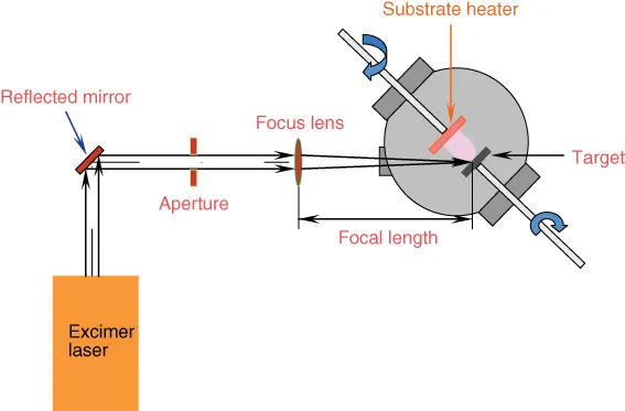
Figure 1.1 Schematic diagram of typical pulsed laser deposition.
1.3 Advantages and Disadvantages of Pulsed Laser Deposition
PLD exhibits many fascinating properties and practical advantages. Firstly, it has the ability to faithfully keep the stoichiometry of the target material, which is the first aspect that draws the attention of the thin film growth community [18]. Secondly, the energy source for material transport (i.e., the laser) is outside the chamber, minimizing any impurities caused by in-vacuum power components; it is very flexible, cost effective, and fast. Many different materials can be ablated by using the same apparatus, and the different laser wavelengths are available in principle. The isolated local heating by the laser spot means that several different materials can be sequentially ablated in a single vacuum chamber by using a carousel system or a segmented target rod to fabricate heterostructures with little of cross-contamination of the source target material. This avoids the interconnected vacuum transfer and is an important advantage in research environment: one laser can serve many vacuum systems in order to save the laser cost, and high-quality samples can be grown in 10 or 20 min. Finally, it is easy to control film thickness and multilayer film by controlling the pulse repetition rate, growth time, and the use of multiple target holders; it demands a much lower substrate temperature than other film deposition techniques because the high kinetic energy (10–100 eV) of species in the ablation plume promotes surface mobility during film growth.
In spite of the above-mentioned advantages of PLD, there are some drawbacks in using the PLD technique. One of the major problems is limited uniformity because the plasma plume ejected from the target can only provide a narrow forward angular distribution. Another problem is high defect or particulate concentration due to surface boiling. The size of particulates may be as large as a few micrometers, which will greatly affect the growth of the subsequent layers as well as the electrical properties of the films. Therefore, these features limit the large-scale film growth. New techniques, such as rotating both target and substra...
Table of contents
- Cover
- Title Page
- Copyright
- Table of Contents
- List of Contributors
- Chapter 1: Pulsed Laser Deposition for Complex Oxide Thin Film and Nanostructure
- Chapter 2: Electron Beam Evaporation Deposition
- Chapter 3: Nanostructures and Thin Films Deposited with Sputtering
- Chapter 4: Nanostructures and Quantum Dots Development with Molecular Beam Epitaxy
- Chapter 5: Carbon Nanomaterials and 2D Layered Materials Development with Chemical Vapor Deposition
- Chapter 6: Nanostructures Development with Atomic Layer Deposition
- Chapter 7: Nanomaterial Development with Liquid-Phase Epitaxy
- Chapter 8: Nanostructural Thin Film Development with Chemical Solution Deposition
- Chapter 9: Nanomaterial Development Using In Situ Liquid Cell Transmission Electron Microscopy
- Chapter 10: Direct-Writing Nanolithography
- Chapter 11: 3D Printing of Nanostructures
- Chapter 12: Nanostructured Thin Film Solid Oxide Fuel Cells
- Chapter 13: Nanostructured Magnetic Thin Films and Coatings
- Chapter 14: Phase Change Materials for Memory Application
- Chapter 15: Nanomaterials and Devices on Flexible Substrates
- Index
- End User License Agreement
Frequently asked questions
Yes, you can cancel anytime from the Subscription tab in your account settings on the Perlego website. Your subscription will stay active until the end of your current billing period. Learn how to cancel your subscription
No, books cannot be downloaded as external files, such as PDFs, for use outside of Perlego. However, you can download books within the Perlego app for offline reading on mobile or tablet. Learn how to download books offline
Perlego offers two plans: Essential and Complete
- Essential is ideal for learners and professionals who enjoy exploring a wide range of subjects. Access the Essential Library with 800,000+ trusted titles and best-sellers across business, personal growth, and the humanities. Includes unlimited reading time and Standard Read Aloud voice.
- Complete: Perfect for advanced learners and researchers needing full, unrestricted access. Unlock 1.5M+ books across hundreds of subjects, including academic and specialized titles. The Complete Plan also includes advanced features like Premium Read Aloud and Research Assistant.
We are an online textbook subscription service, where you can get access to an entire online library for less than the price of a single book per month. With over 1.5 million books across 990+ topics, we’ve got you covered! Learn about our mission
Look out for the read-aloud symbol on your next book to see if you can listen to it. The read-aloud tool reads text aloud for you, highlighting the text as it is being read. You can pause it, speed it up and slow it down. Learn more about Read Aloud
Yes! You can use the Perlego app on both iOS and Android devices to read anytime, anywhere — even offline. Perfect for commutes or when you’re on the go.
Please note we cannot support devices running on iOS 13 and Android 7 or earlier. Learn more about using the app
Please note we cannot support devices running on iOS 13 and Android 7 or earlier. Learn more about using the app
Yes, you can access Advanced Nano Deposition Methods by Yuan Lin in PDF and/or ePUB format, as well as other popular books in Technology & Engineering & Materials Science. We have over 1.5 million books available in our catalogue for you to explore.