Edited by key figures in 3D integration and written by top authors from high-tech companies and renowned research institutions, this book covers the intricate details of 3D process technology. As such, the main focus is on silicon via formation, bonding and debonding, thinning, via reveal and backside processing, both from a technological and a materials science perspective. The last part of the book is concerned with assessing and enhancing the reliability of the 3D integrated devices, which is a prerequisite for the large-scale implementation of this emerging technology.
Invaluable reading for materials scientists, semiconductor physicists, and those working in the semiconductor industry, as well as IT and electrical engineers.
eBook - ePub
Handbook of 3D Integration, Volume 3
3D Process Technology
- English
- ePUB (mobile friendly)
- Available on iOS & Android
eBook - ePub
Handbook of 3D Integration, Volume 3
3D Process Technology
About this book
Trusted by 375,005 students
Access to over 1.5 million titles for a fair monthly price.
Study more efficiently using our study tools.
Information
1
3D IC Integration Since 2008
Philip Garrou, Peter Ramm, and Mitsumasa Koyanagi
In Volume 1, we covered some of the history of the development of the 3D integrated circuit (3D IC) concept and we direct you to that chapter for such content [1].
Since the first two volumes of the Handbook of 3D Integration appeared in 2008, significant progress has been made to bring 3D IC technology to commercialization. This chapter will attempt to summarize some of the key developments during that period.
We previously described 3D IC integration as “an emerging, system level integration architecture wherein multiple strata (layers) of planar devices are stacked and interconnected using through-silicon (or other semiconductor material) vias (TSV) in the Z direction” as depicted schematically in Figure 1.1a and in cross section in Figure 1.1b [1].
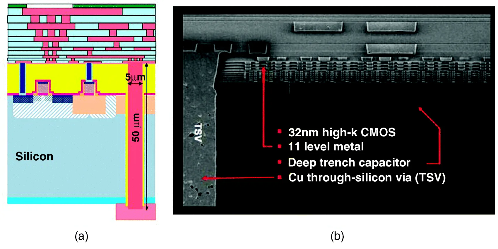
Figure 1.1 3D IC with TSV: (a) schematic (courtesy of IMEC) and (b) cross section (courtesy of IBM). Note that the IBM cross section is connected at a higher (fatter) on chip interconnect level.
With the continued pressure to miniaturize portable products and the near universal agreement that scaling as we have known it is soon coming to an end [2], a perfect storm has been created. The response to this dilemma at both the device and the package level has been to move into the third dimension.
It is commonly accepted that chip stacks wire-bonded down to a common laminate base and stacked packages such as package-on-package (PoP) are categorized as “3D packaging.” Transistor design has also gone vertical [3] as Intel [4] and others move to “finfet” stacked transistor structures at the 22 nm generation. These are compared pictorially in Figure 1.2.
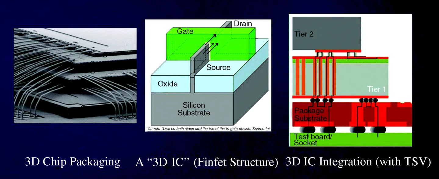
Figure 1.2 3D packaging, 3D finfet transistors, and 3D IC integration.
In Figure 1.3, we compare system-on-chip (SoC), 3D packaging, and 3D IC with through-silicon via (TSV) in various performance categories [5].
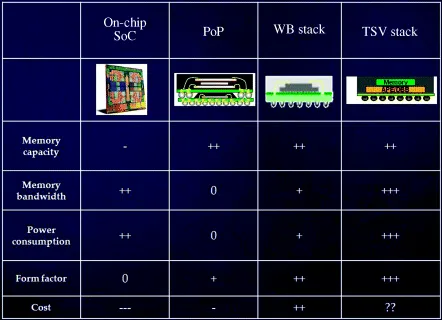
Figure 1.3 Comparison of SoC, 3D packaging, and 3D IC [5].
1.1 3D IC Nomenclature
Since 2008 there have been attempts to further refine the nomenclature for 3D IC integration, although it has not yet been universally adopted in publications. In 2009 the International Technology Roadmap for Semiconductors (ITRS) proposed the following nomenclature in an attempt to define the possible different levels of connections possible as circuits are deconstructed onto separate strata (see Table 1.1) [6].
Table 1.1 2009 ITRS roadmap [6]
| Level | Suggested name | Supply chain | Key characteristics |
| Package | 3D packaging (3D-P) | OSAT assembly printed circuit board (PCB) |
|
| Bond-pad | 3D wafer-level package (3D-WLP) | Wafer-level packaging |
|
| Global | 3D stacked integrated circuit/3D system-on-chip (3D-SIC/3D-SoC) | Wafer fab |
|
Table of contents
- Cover
- Related Titles
- Title Page
- Copyright
- List of Contributors
- Chapter 1: 3D IC Integration Since 2008
- Chapter 2: Key Applications and Market Trends for 3D Integration and Interposer Technologies
- Chapter 3: Economic Drivers and Impediments for 2.5D/3D Integration
- Chapter 4: Interposer Technology
- Chapter 5: TSV Formation Overview
- Chapter 6: TSV Unit Processes and Integration
- Chapter 7: TSV Formation at ASET
- Chapter 8: Laser-Assisted Wafer Processing: New Perspectives in Through-Substrate Via Drilling and Redistribution Layer Deposition
- Chapter 9: Temporary Bonding Material Requirements
- Chapter 10: Temporary Bonding and Debonding – An Update on Materials and Methods
- Chapter 11: ZoneBOND®: Recent Developments in Temporary Bonding and Room-Temperature Debonding
- Chapter 12: Temporary Bonding and Debonding at TOK
- Chapter 13: The 3M™ Wafer Support System (WSS)
- Chapter 14: Comparison of Temporary Bonding and Debonding Process Flows
- Chapter 15: Thinning, Via Reveal, and Backside Processing – Overview
- Chapter 16: Backside Thinning and Stress-Relief Techniques for Thin Silicon Wafers
- Chapter 17: Via Reveal and Backside Processing
- Chapter 18: Dicing, Grinding, and Polishing (Kiru Kezuru and Migaku)
- Chapter 19: Overview of Bonding and Assembly for 3D Integration
- Chapter 20: Bonding and Assembly at TSMC
- Chapter 21: TSV Packaging Development at STATS ChipPAC
- Chapter 22: Cu–SiO2 Hybrid Bonding
- Chapter 23: Bump Interconnect for 2.5D and 3D Integration
- Chapter 24: Self-Assembly Based 3D and Heterointegration
- Chapter 25: High-Accuracy Self-Alignment of Thin Silicon Dies on Plasma-Programmed Surfaces
- Chapter 26: Challenges in 3D Fabrication
- Chapter 27: Cu TSV Stress: Avoiding Cu Protrusion and Impact on Devices
- Chapter 28: Implications of Stress/Strain and Metal Contamination on Thinned Die
- Chapter 29: Metrology Needs for 2.5D/3D Interconnects
- Index
- End User License Agreement
Frequently asked questions
Yes, you can cancel anytime from the Subscription tab in your account settings on the Perlego website. Your subscription will stay active until the end of your current billing period. Learn how to cancel your subscription
No, books cannot be downloaded as external files, such as PDFs, for use outside of Perlego. However, you can download books within the Perlego app for offline reading on mobile or tablet. Learn how to download books offline
Perlego offers two plans: Essential and Complete
- Essential is ideal for learners and professionals who enjoy exploring a wide range of subjects. Access the Essential Library with 800,000+ trusted titles and best-sellers across business, personal growth, and the humanities. Includes unlimited reading time and Standard Read Aloud voice.
- Complete: Perfect for advanced learners and researchers needing full, unrestricted access. Unlock 1.5M+ books across hundreds of subjects, including academic and specialized titles. The Complete Plan also includes advanced features like Premium Read Aloud and Research Assistant.
We are an online textbook subscription service, where you can get access to an entire online library for less than the price of a single book per month. With over 1.5 million books across 990+ topics, we’ve got you covered! Learn about our mission
Look out for the read-aloud symbol on your next book to see if you can listen to it. The read-aloud tool reads text aloud for you, highlighting the text as it is being read. You can pause it, speed it up and slow it down. Learn more about Read Aloud
Yes! You can use the Perlego app on both iOS and Android devices to read anytime, anywhere — even offline. Perfect for commutes or when you’re on the go.
Please note we cannot support devices running on iOS 13 and Android 7 or earlier. Learn more about using the app
Please note we cannot support devices running on iOS 13 and Android 7 or earlier. Learn more about using the app
Yes, you can access Handbook of 3D Integration, Volume 3 by Philip Garrou, Mitsumasa Koyanagi, Peter Ramm, Philip Garrou,Mitsumasa Koyanagi,Peter Ramm in PDF and/or ePUB format, as well as other popular books in Technology & Engineering & Materials Science. We have over 1.5 million books available in our catalogue for you to explore.