Advances in Embedded and Fan-Out Wafer Level Packaging Technologies
eBook - ePub

Advances in Embedded and Fan-Out Wafer Level Packaging Technologies

  1. English
  2. ePUB (mobile friendly)
  3. Available on iOS & Android
eBook - ePub

Advances in Embedded and Fan-Out Wafer Level Packaging Technologies

About this book

Examines the advantages of Embedded and FO-WLP technologies, potential application spaces, package structures available in the industry, process flows, and material challenges

Embedded and fan-out wafer level packaging (FO-WLP) technologies have been developed across the industry over the past 15 years and have been in high volume manufacturing for nearly a decade. This book covers the advances that have been made in this new packaging technology and discusses the many benefits it provides to the electronic packaging industry and supply chain. It provides a compact overview of the major types of technologies offered in this field, on what is available, how it is processed, what is driving its development, and the pros and cons.

Filled with contributions from some of the field's leading experts, Advances in Embedded and Fan-Out Wafer Level Packaging Technologies begins with a look at the history of the technology. It then goes on to examine the biggest technology and marketing trends. Other sections are dedicated to chip-first FO-WLP, chip-last FO-WLP, embedded die packaging, materials challenges, equipment challenges, and resulting technology fusions.

  • Discusses specific company standards and their development results
  • Content relates to practice as well as to contemporary and future challenges in electronics system integration and packaging

Advances in Embedded and Fan-Out Wafer Level Packaging Technologies will appeal to microelectronic packaging engineers, managers, and decision makers working in OEMs, IDMs, IFMs, OSATs, silicon foundries, materials suppliers, equipment suppliers, and CAD tool suppliers. It is also an excellent book for professors and graduate students working in microelectronic packaging research.

Frequently asked questions

Yes, you can cancel anytime from the Subscription tab in your account settings on the Perlego website. Your subscription will stay active until the end of your current billing period. Learn how to cancel your subscription.
No, books cannot be downloaded as external files, such as PDFs, for use outside of Perlego. However, you can download books within the Perlego app for offline reading on mobile or tablet. Learn more here.
Perlego offers two plans: Essential and Complete
  • Essential is ideal for learners and professionals who enjoy exploring a wide range of subjects. Access the Essential Library with 800,000+ trusted titles and best-sellers across business, personal growth, and the humanities. Includes unlimited reading time and Standard Read Aloud voice.
  • Complete: Perfect for advanced learners and researchers needing full, unrestricted access. Unlock 1.4M+ books across hundreds of subjects, including academic and specialized titles. The Complete Plan also includes advanced features like Premium Read Aloud and Research Assistant.
Both plans are available with monthly, semester, or annual billing cycles.
We are an online textbook subscription service, where you can get access to an entire online library for less than the price of a single book per month. With over 1 million books across 1000+ topics, we’ve got you covered! Learn more here.
Look out for the read-aloud symbol on your next book to see if you can listen to it. The read-aloud tool reads text aloud for you, highlighting the text as it is being read. You can pause it, speed it up and slow it down. Learn more here.
Yes! You can use the Perlego app on both iOS or Android devices to read anytime, anywhere — even offline. Perfect for commutes or when you’re on the go.
Please note we cannot support devices running on iOS 13 and Android 7 or earlier. Learn more about using the app.
Yes, you can access Advances in Embedded and Fan-Out Wafer Level Packaging Technologies by Beth Keser, Steffen Kröhnert, Beth Keser,Steffen Kroehnert, Beth Keser, Steffen Kroehnert in PDF and/or ePUB format, as well as other popular books in Tecnologia e ingegneria & Ingegneria elettronica e telecomunicazioni. We have over one million books available in our catalogue for you to explore.

1
History of Embedded and Fan‐Out Packaging Technology

Michael Töpper, Andreas Ostmann, Tanja Braun, and Klaus‐Dieter Lang
Fraunhofer IZM, Berlin, Germany

1.1 Introduction

The fabrication of microelectronic systems purely monolithically on a wafer is limited by the need for mixed technologies and redundancy. Multi‐chip modules (MCMs) provided an alternative in achieving high density interconnects (HDI) being originally developed in the 1980s for aerospace applications, where size and weight were critical requirements [1]. The core idea of MCM was therefore the reduction of the interconnection length between different electronic components like integrated circuits (ICs), passives, and others like optoelectronic components. In 1990, silicon devices of 16 mm × 16 mm were the limits of manufacturability in volume production – far from the wafer‐scale integration goals necessary for large electronic systems. Therefore, multiple ICs were needed, which resulted in a hybrid manufacturing process. Standard packaging technologies have used single packaged ICs that are mounted on the printed circuit board (PCB). The electrical signals have to travel from the IC through the package and through the PCB to the next package, limiting the high‐speed performance of the systems. This translates to long interconnection lengths between devices and a corresponding increase in propagation delay. MCM was the first approach to eliminate the package and to use a high density routing substrate instead of PCB. All ICs and also the substrates can be pretested to ensure a high yield module process.
The interconnection of the bare ICs to the MCM substrate can be done by direct chip connection using wire bonding (WB), tape‐automated bonding (TAB), or flip‐chip (FC) bonding. The basic MCM concept was first proposed by IBM in 1972 as an “active silicon chip carrier” [2]. There were three main approaches for MCM processes developed: MCM‐laminate (MCM‐L), in which a multilayer prepreg laminated board was used; high density ceramic MCM (MCM‐C), in which a multilayer co‐fired ceramic substrate was used; and thin film deposited MCM (MCM‐D), in which a thin film metal/dielectric substrate was used. The reason for building MCM‐D in the late 1980s will still sound familiar today: providing off‐the‐chip interconnect bandwidth matching the semiconductors clocking rates, decreasing power dissipation in input and output (I/O) drivers with matched impedance, and reducing the volume and size of the circuits. The difference between then and now is a major push for low fabrication costs to satisfy the consumer markets. System in packages (SiP) can therefore be viewed as an extension of an MCM. In addition, the lack of availability of known good die (KGD) for the different applications was a major hurdle to get functional MCMs with a sufficient yield. All of these types were in principle “chip‐last” technologies in which the interconnection substrate is manufactured before the chip attachment being done by FC, WB, or less used TAB. “Chip‐first” is the usage of an embedding process where the chips are placed under the interconnection layer. The chips have to be placed onto or within a base substrate prior to the fabrication of the interconnect structure that is then a direct metallurgical contact eliminating FC, WB, or TAB. With such an electrical interconnect, a reference ground plane can be deposited directly onto the chip pads, which provide a very well‐matched high frequency interconnect structure. The inductance and the capacitance are over 10 times lower compared with FC, TAB, and WB.
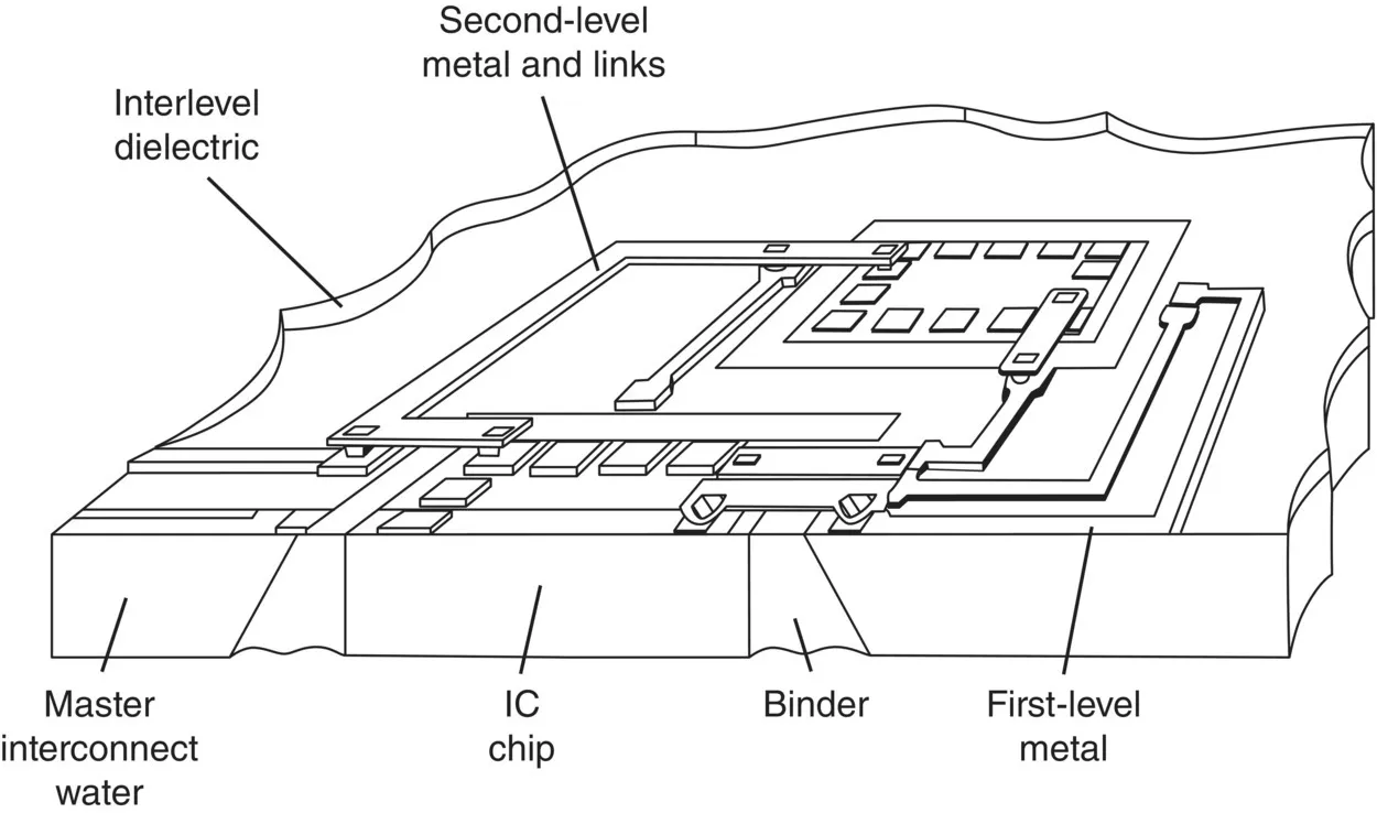
Therefore embedding‐type MCMs have been developed to bypass the yield issue for monolithic wafer‐scale integration. Main pioneering work was done by Wayne Johnson from Auburn University and Ray Fillion from GE Research. Johnson et al. proposed a hybrid that uses pretested ICs mounted into cavities etched in a silicon wafer [3]. A schematic of this concept is shown in Figure 1.1.
Schematic of an embedded MCM with lines indicating master interconnect water, IC chip, binder, first-level metal, interlevel dielectric, and second-level metal and links.
Figure 1.1 Schematic of an embedded MCM proposed by Johnson et al. [3].
Source: Reproduced with permission of IEEE.
The chips are interconnected with planar thin film process steps. An additional metallization layer is used for the interconnection to the next packaging hierarchy. The cavity is etched anisotropically into a silicon wafer using standard MEMS technology, which gives 54.74° sidewall angles. A 15 μm thin Si membrane was left to facilitate the deposition of the metal routing on the top Si surface. This membrane was removed by dry etching before chip embedding. The components are inserted from the backside and glued inside the thermally oxidized Si carrier with an adhesive (epoxy resin with 75% inorganic filler). In one of these first embedding approaches, benzocyclobutene (BCB) was deposited on top of the Si wafer containing four ICs for planarizing the surface of the substrate for the subsequent routing process. The low curing temperature is of great benefit for this embedding‐type approach due to the low thermal stability of the epoxy resin used for gap filling. After curing the BCB was structured by reactive ion etching (RIE). To correct for chip‐to‐wafer misalignment occurring during die mounting from the backside of the substrate, a computer program was written that automatically calculated a corrected pattern generator file for mask making.
An even earlier approach for embedding was patented in 1968 by Ties Siebolt Te Velde and Albert Schmitz from Philips...

Table of contents

  1. Cover
  2. Table of Contents
  3. Preface
  4. List of Contributors
  5. Acknowledgments
  6. 1 History of Embedded and Fan‐Out Packaging Technology
  7. 2 FO‐WLP Market and Technology Trends
  8. 3 Embedded Wafer‐Level Ball Grid Array (eWLB) Packaging Technology Platform
  9. 4 Ultrathin 3D FO‐WLP eWLB‐PoP (Embedded Wafer‐Level Ball Grid Array‐Package‐on‐Package) Technology
  10. 5 NEPES’ Fan‐Out Packaging Technology from Single die, SiP to Panel‐Level Packaging
  11. 6 M‐Series™ Fan‐Out with Adaptive Patterning™
  12. 7 SWIFT® Semiconductor Packaging Technology
  13. 8 Embedded Silicon Fan‐Out (eSiFO®) Technology for Wafer‐Level System Integration
  14. 9 Embedding of Active and Passive Devices by Using an Embedded Interposer: The i2 Board Technology
  15. 10 Embedding of Power Electronic Components: The Smart p2 Pack Technology
  16. 11 Embedded Die in Substrate (Panel‐Level) Packaging Technology
  17. 12 Blade: A Chip‐First Embedded Technology for Power Packaging
  18. 13 The Role of Liquid Molding Compounds in the Success of Fan‐Out Wafer‐Level Packaging Technology
  19. 14 Advanced Dielectric Materials (Polyimides and Polybenzoxazoles) for Fan‐Out Wafer‐Level Packaging (FO‐WLP)
  20. 15 Enabling Low Temperature Cure Dielectrics for Advanced Wafer‐Level Packaging
  21. 16 The Role of Pick and Place in Fan‐Out Wafer‐Level Packaging
  22. 17 Process and Equipment for eWLB: Chip Embedding by Molding
  23. 18 Tools for Fan‐Out Wafer‐Level Package Processing
  24. 19 Equipment and Process for eWLB: Required PVD/Sputter Solutions
  25. 20 Excimer Laser Ablation for the Patterning of Ultra‐fine Routings
  26. 21 Temporary Carrier Technologies for eWLB and RDL‐First Fan‐Out Wafer‐Level Packages
  27. 22 Encapsulated Wafer‐Level Package Technology (eWLCSP): Robust WLCSP Reliability with Sidewall Protection
  28. 23 Embedded Multi‐die Interconnect Bridge (EMIB): A Localized, High Density, High Bandwidth Packaging Interconnect
  29. 24 Interconnection Technology Innovations in2.5D Integrated Electronic Systems
  30. Index
  31. End User License Agreement