Helps readers understand the physics behind MOS devices for low-voltage and low-energy applications
- Based on timely published and unpublished work written by expert authors
- Discusses various promising MOS devices applicable to low-energy environmental and biomedical uses
- Describes the physical effects (quantum, tunneling) of MOS devices
- Demonstrates the performance of devices, helping readers to choose right devices applicable to an industrial or consumer environment
- Addresses some Ge-based devices and other compound-material-based devices for high-frequency applications and future development of high performance devices.
"Seemingly innocuous everyday devices such as smartphones, tablets and services such as on-line gaming or internet keyword searches consume vast amounts of energy. Even when in standby mode, all these devices consume energy. The upcoming 'Internet of Things' (IoT) is expected to deploy 60 billion electronic devices spread out in our homes, cars and cities.
Britain is already consuming up to 16 per cent of all its power through internet use and this rate is doubling every four years. According to The UK's Daily Mail May (2015), if usage rates continue, all of Britain's power supply could be consumed by internet use in just 20 years. In 2013, U.S. data centers consumed an estimated 91 billion kilowatt-hours of electricity, corresponding to the power generated by seventeen 1000-megawatt nuclear power plants. Data center electricity consumption is projected to increase to roughly 140 billion kilowatt-hours annually by 2020, the equivalent annual output of 50 nuclear power plants."
—Natural Resources Defense Council, USA, Feb. 2015
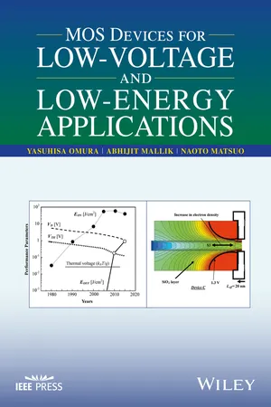
All these examples stress the urgent need for developing electronic devices that consume as little energy as possible. The book "MOS Devices for Low-Voltage and Low-Energy Applications" explores the different transistor options that can be utilized to achieve that goal. It describes in detail the physics and performance of transistors that can be operated at low voltage and consume little power, such as subthreshold operation in bulk transistors, fully depleted SOI devices, tunnel FETs, multigate and gate-all-around MOSFETs. Examples of low-energy circuits making use of these devices are given as well.
"The book MOS Devices for Low-Voltage and Low-Energy Applications is a good reference for graduate students, researchers, semiconductor and electrical engineers who will design the electronic systems of tomorrow."
—Dr. Jean-Pierre Colinge, Taiwan Semiconductor Manufacturing Company (TSMC)
"The authors present a creative way to show how different MOS devices can be used for low-voltage and low-power applications. They start with Bulk MOSFET, following with SOI MOSFET, FinFET, gate-all-around MOSFET, Tunnel-FET and others. It is presented the physics behind the devices, models, simulations, experimental results and applications. This book is interesting for researchers, graduate and undergraduate students. The low-energy field is an important topic for integrated circuits in the future and none can stay out of this."
—Prof. Joao A. Martino, University of Sao Paulo, Brazil