![]()
Chapter 1
Carbon as a MEMS Material
Amritha Rammohan* and Ashutosh Sharma
Department of Chemical Engineering, Indian Institute of Technology, Kanpur, Uttar Pradesh, India
Abstract
Carbon has become a popular material in microelectromechanical (MEMS) applications because of its versatile electrochemical and mechanical properties, as well as the numerous precursor materials and facile fabrication methods available. This review details various C-MEMS fabrication technologies, most of which involve the patterning of polymeric precursors of carbon such as epoxy photoresists and sol–gel polymers followed by their pyrolysis to create glassy or semicrystalline carbon pattern replicas. The structure and properties of glassy carbon, as well as the pyrolysis process and concurrent shrinkage, are also discussed in detail, as these directly affect the applicability of the carbon structures and devices. The integration of carbon structures in MEMS devices by means of surface modification and the incorporation of additives and fillers such as carbon nanotubes and carbon nanofibers to enhance the functional properties are also discussed.
Keywords: Carbon, C-MEMS, pyrolysis, volumetric shrinkage, MEMS integration, lithography
1.1 Introduction
Carbon is one of the most versatile materials in the periodic table. Due to its ability to form sp, sp2, and sp3 hybridized covalent bonds with various elements including itself, carbon-based compounds and materials are amongst the most adaptable materials available to us. The ability of carbon to form bonds with itself is manifested in the form of many allotropes of carbon including fullerenes, nanotubes, graphite, graphene, and diamond. Even within these allotropes, despite being all made of carbon, the properties such as electrical conductivity, hardness, and strength vary widely with allotrope due to different microstructures in terms of crystallite size, long-range order, anisotropy, etc. [1]. Amorphous or glassy carbon, in particular, has a wide window of electrochemical stability as well as high thermal conductivity and excellent biocompatibility, warranting its use in various electrochemical and biological applications [2]. Diamond-like carbon or DLC, another form of carbon, has superior tribological properties and wear resistance, and anisotropic carbon materials such as nanotubes and nanofibers can be leveraged for their unique and anisotropic electromechanical properties as well [2–4].
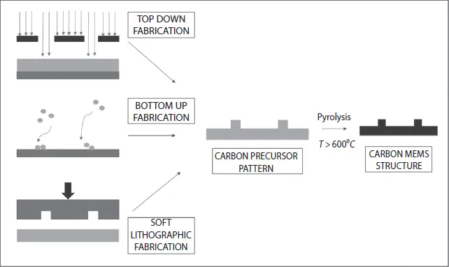
When this versatility in functional properties is combined with appropriate micro/nanofabrication techniques, carbon structures become highly viable as elements in micro and nano electromechanical systems (MEMS/NEMS). In order to create micro- and nanosized electromechanical structures such as actuators and microsensors from carbon, appropriate robust and facile micro/nanofabrication techniques have to be adopted. The methods to pattern carbon and its precursors into MEMS structures are divided, like other microfabrication techniques, into top-down and bottom-up techniques. Top-down techniques are subtractive processes such as reactive ion etching (RIE) and lithographic patterning with photons, electrons, or ions. Bottom-up or additive processes include sputtering, evaporation, and chemical vapor deposition (CVD) [5]. While top-down techniques create deterministic patterns with good shape and size control, bottom-up techniques result in increased functionality and have greater capability for three-dimensional (3D) patterns. Self-assembled structures that are formed with very little external guidance or direction also fall in the latter category of bottom-up techniques. Apart from strictly top-down and bottom-up techniques, many fabrication techniques include a combination of these two. For example, hierarchical structures can be achieved by top-down patterning of large-scale structures and bottom-up patterning of smaller, 3D features. Soft lithographic techniques such as micromolding and nanoimprinting are often considered a third classification of microfabrication techniques and have also been used successfully in the patterning of C-MEMS (Carbon MEMS) structures [6].
One process that facilitates the fabrication of amorphous or glassy carbon microstructures involves the pyrolysis of carbon-containing precursor molecules (usually polymers) that have been prefabricated into requisite micro/nanostructures (Figure 1.1). Pyrolysis or carbonization is the method of heating carbon-containing precursors to temperatures upward of 600 °C in an inert atmosphere such as nitrogen or argon to remove noncarbonaceous components in a material by volatilizing them into gaseous and hence removable compounds. This method, apart from allowing the creation of any required shape as long as appropriate formable precursors are used, also allows tweaking the properties of the final carbon micro/nanostructures by the rational use of various precursors with different functional groups. Appropriate precursors are those carbon-containing polymers that result in a high enough yield of carbonaceous residue and at the same time do not reflow when subjected to high temperatures during pyrolysis [2]. Thus, the methods to create glassy carbon MEMS structures can be decoupled into various methods to create microstructures in appropriate precursors and the pyrolysis processes (Figure 1.1).
This review is structured as follows. Due to the fact that majority of C-MEMS/NEMS processes involve polymer-derived amorphous or semicrystalline carbon, its properties are reviewed and contrasted with other MEMS materials. The process of pyrolysis for the carbonization is discussed in detail along with methods to address the issue of shrinkage. Then, lithographic techniques and their capabilities and modifications for C-MEMS/NEMS fabrication are discussed. This is followed by a description of bottom-up techniques, in particular self-assembly techniques for C-MEMS/NEMS. Soft lithographic techniques are also briefly covered. Finally, additives and surface modification techniques to improve and expand the applicability of carbon are examined.
1.2 Structure and Properties of Glassy Carbon
Glassy carbon is typically a hard solid prepared by treating polymeric precursors such as copolymer resins at elevated temperatures (600–3000 °C) having increasing amount of graphitic content with increasing temperature. The high temperature removes almost all of the noncarbon elements present in the polymers leaving behind a carbonaceous residue. A fully graphitic material does not develop in usual pyrolysis due to the difficulty in breaking the C–C bonds in the parent polymeric chains as well as other factors such as ratio of sp2 to sp3 carbon atoms and amount of hydrogen present in the precursor. The structure is generally understood as entangled ribbons of graphitic planes containing small isolated crystals of graphite. When characterized by Raman spectroscopy, two first-order bands around 1360 cm−1 (D band) and 1580 cm−1 (G band) are usually observed, which indicate the defect-induced, double-resonance scattering and symmetry in-plane stretching of graphite, respectively. Weak second-order bands related to the 3D ordering of graphite may also be observed between 2700 and 2900 cm−1. It is important to note that the D band mainly arises due to the finite graphite crystallite size and associated defects [7]. As glassy carbon contains smaller crystallites of graphite, its density is less than that of graphite and can be applied in applications requiring lightweight yet chemically inert or thermally stable materials.
While the different preparation methods result in a range of physical properties of glassy carbon, it does have many advantages as a MEMS material. Glassy carbon, for instance, has a lower Young’s modulus compared to silicon (10–40 GPa compared to 40–190 GPa for silicon) and a lower surface energy. Thus, carbon can be used in MEMS actuators or other devices where high stiffness is detrimental. The lower surface energy of carbon also solves the problem of stiction in contacting or proximal MEMS elements where capillary forces cause sticking between close surfaces. Carbon resulting from pyrolysis is also rather inert and impervious in many corrosive chemical environments. It is also possible to tailor the porosity and functionalize the surface of glassy carbon using various carbon chemistry routes as illustrated in Section 1.4.
Glassy carbon is also a model material or gold standard for electrochemists to compare the electrochemical properties of electrodes of other materials as it exhibits excellent electrochemical properties. The electrochemical and physical properties of photoresist material pyrolyzed at temperatures between 600 °C and 1100 °C have been studied in detail, and it has been found that resistance of the material is lower and the electrochemical performance of the carbon material is often found to be better. The pyrolyzed positive photoresist (eg. AZ 4330) films have low capacitance as well as background current [8].
Apart from glassy carbon, other carbon-based materials such as DLC, carbon nanotubes (CNTs), and carbon nanofibers (CNFs) have also been applied to great benefit in MEMS devices. However, these materials often lack the capability to form the entire MEMS device by themselves due to fabrication and manipulation constraints. For instance, while DLC is particularly useful as a coating material to improve the wear resistance, reduce friction, and stiction in contacting microcomponents in MEMS devices, the residual stresses that are created in most of the high-energy techniques involved in DLC fabrication often lead to delamination of thicker DLC films precluding their use as structural elements [3]. CNTs and CNFs have unique and anisotropic thermal and electrochemical properties and have been used as structural elements such as cantilevers and microsensors. However, the manipulation and assembly of fabricated CNTs and CNFs on MEMS devices are nontrivial due the possibility of physical damage or morphological changes occurring. Cook and Carter [9] have recently reviewed the effect of different MEMS processes on arc-discharge produced and catalytically grown multiwall CNTs (MWCNTs) and found that while CVD deposition of other materials is compatible with MWCNTs, plasma etching processes tend to cause significant damage. Dau et al. [10] have been able to manually maneuver CVD-grown CNT films onto a substrate and pattern it using e-beam lithography into a mechanical sensor. It is also possible to directly synthesize patterned CNT structures for MEMS applications by methods such as CVD on patterned catalyst substrates [11–14], direct or post-synthetic patterning [15–18], templated deposition [19], etc. The incorporation of CNTs and CNFs into C-MEMS devices can be as fillers or (surface) additives to enhance useful properties or as structural elements integrated with the rest of the device. Both these uses are discussed in Section 1.4.
1.3 Fabrication of C-MEMS Structures
1.3.1 Mechanism and Features of the Pyrolysis Process
As most C-MEMS processes involve the use of pyrolysis, also known as carbonization, for the conversion of precursors to carbon, a good understanding of this process is a prerequisite for understanding C-MEMS fabrication. Pyrolysis, from the Greek for fire (pyro) and separation (lysis), is the thermochemical decomposition of a material and in the context of carbonization refers to the breakdown of carbon-containing precursors at el...