- Offers a comprehensive overview of NAND flash memories, with insights into NAND history, technology, challenges, evolutions, and perspectives
- Describes new program disturb issues, data retention, power consumption, and possible solutions for the challenges of 3D NAND flash memory
- Written by an authority in NAND flash memory technology, with over 25 years' experience
- English
- ePUB (mobile friendly)
- Available on iOS & Android
eBook - ePub
NAND Flash Memory Technologies
About this book
Trusted by 375,005 students
Access to over 1.5 million titles for a fair monthly price.
Study more efficiently using our study tools.
Information
1
INTRODUCTION
1.1 Background
Recent progress in computers and mobile equipment requires further efforts in developing higher-density nonvolatile semiconductor memories. A breakthrough in the field of nonvolatile memories was the invention of the flash memory [1], which is a new type of EEPROM (electrically erasable and programmable read-only memory), as shown in Fig. 1.1a. The first paper discussing the flash memory was presented in 1984 IEDM (International Electron Device Meeting). The flash memory has many advantages in comparison with other nonvolatile memories. Therefore, the flash memory explosively accelerated the development of higher-density EEPROMs.
In 1987, a NAND structured cell was proposed by Masuoka et al. [2]. This structure can reduce the memory cell size without scaling of device dimension. The NAND structure cell arranges a number of bits in series, as shown in Fig. 1.1b [2]. The conventional EPROM cell has one contact area per two bits. However, for a NAND structure cell, only one contact hole is required per two NAND structure cells (NAND string). As a result, the NAND cell can realize a smaller cell area per bit than the conventional EPROM.
Applications of flash memory became quite wide due to nonvolatility, fast access, and robustness. Flash memory application can be classified into two major markets (Fig. 1.1). One is for code storage applications, such as PC BIOS, cellular phones, and DVDs. The NOR-type cell is best suitable for this market due to its fast random access speed. The other is for file storage applications, such as the digital still camera (DSC), silicon audio, the smartphone, and the tablet PC. The NAND-type cell is suitable for file storage market.
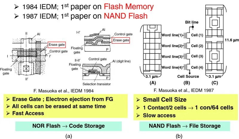
FIGURE 1.1 Invention of flash memory and NAND flash memory. (a) Flash memory. All cells in the memory chip can be erased at the same time by applying erase voltage to the erase gate [1]. (b) NAND flash memory [2]. Memory cells are connected in series to share contact area. Comparison between (A) NAND cell and (C) conventional EPROM (NOR flash cell). (B) shows the equivalent circuit of the NAND structure cell having 4 cells.
Figure 1.2 shows the memory hierarchy of computer system before mass production of NAND Flash. SRAM and DRAM had been used as cash memory and main memory, respectively. And magnetic memories, such as HDD, had been used as a nonvolatile mass-storage device. NAND flash memory had been targeted to replace magnetic memory [54]. Actually, from the production start of NAND flash memory in 1992, the NAND flash memory has been widely applied to new emerging applications and has replaced magnetic memory, as shown in Fig. 1.3. At first, a photo film had been completely replaced by the memory cards of NAND flash memory. Next, the floppy disk was replaced by USB drive memory. The mobile music equipment with cassette tape was replaced by the MP3 player using flash memory storage. Also, NAND flash memory had created new market of smartphones and tablet PCs. And now, the application is extending to the SSD (solid-state drive) market, not only for the consumer but also for the enterprise server. Therefore, over 20 years, NAND flash memory has created new large-volume markets and industries of consumer, computer, mass storage, and enterprise server. NAND flash production volume was tremendously increased. The overall NAND market is expected to reach $40 billion in 2016 [55]. NAND flash has become an explosive innovation and has greatly contributed to the improvement of our lives with the advent of convenient mobile equipment such as smartphones and tablet PCs.
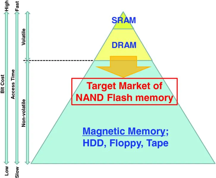
FIGURE 1.2 Target market of NAND flash memory.
Table 1.1 shows the history of NAND flash memory development, based on technical papers from 1987 to 1997. During the 10 years from the first NAND flash paper in 1987, all of the fundamental and important NAND flash technologies were established, such as page programming [7, 8], block erase, the uniform program and uniform well erase scheme [9, 12, 13], bit-by-bit verify [15, 21], the ISPP (incremental step pulse program) [25, 26, 29], the self-aligned STI cell [22, 51, 56], the shield bit-line scheme [21], and so on. These technologies could satisfy the requirements of file storage memory.
Table 1.1 History of the NAND Flash Memory (∼1997)
| Year | Authors | References | Conference/Journal | |
| 1984 | Flash Memory, first paper | F. Masuoka et al. | [1] | IEDM 1984 |
| 1987 | NAND-typ... |
Table of contents
- Cover
- IEEE Press
- TitlePage
- Copyright
- Foreword
- Preface
- Acknowledgments
- About the Author
- 1 Introduction
- 2 Principle of NAND Flash Memory
- 3 NAND Flash Memory Devices
- 4 Advanced Operation for Multilevel Cell
- 5 Scaling Challenge of NAND Flash Memory Cells
- 6 Reliability of NAND Flash Memory
- 7 Three-Dimensional NAND Flash Cell
- 8 Challenges of Three-Dimensional NAND Flash Memory
- 9 Conclusions
- Index
- IEEE Press Series on Microelectronic Systems
- EULA
Frequently asked questions
Yes, you can cancel anytime from the Subscription tab in your account settings on the Perlego website. Your subscription will stay active until the end of your current billing period. Learn how to cancel your subscription
No, books cannot be downloaded as external files, such as PDFs, for use outside of Perlego. However, you can download books within the Perlego app for offline reading on mobile or tablet. Learn how to download books offline
Perlego offers two plans: Essential and Complete
- Essential is ideal for learners and professionals who enjoy exploring a wide range of subjects. Access the Essential Library with 800,000+ trusted titles and best-sellers across business, personal growth, and the humanities. Includes unlimited reading time and Standard Read Aloud voice.
- Complete: Perfect for advanced learners and researchers needing full, unrestricted access. Unlock 1.5M+ books across hundreds of subjects, including academic and specialized titles. The Complete Plan also includes advanced features like Premium Read Aloud and Research Assistant.
We are an online textbook subscription service, where you can get access to an entire online library for less than the price of a single book per month. With over 1.5 million books across 990+ topics, we’ve got you covered! Learn about our mission
Look out for the read-aloud symbol on your next book to see if you can listen to it. The read-aloud tool reads text aloud for you, highlighting the text as it is being read. You can pause it, speed it up and slow it down. Learn more about Read Aloud
Yes! You can use the Perlego app on both iOS and Android devices to read anytime, anywhere — even offline. Perfect for commutes or when you’re on the go.
Please note we cannot support devices running on iOS 13 and Android 7 or earlier. Learn more about using the app
Please note we cannot support devices running on iOS 13 and Android 7 or earlier. Learn more about using the app
Yes, you can access NAND Flash Memory Technologies by Seiichi Aritome in PDF and/or ePUB format, as well as other popular books in Technology & Engineering & Electrical Engineering & Telecommunications. We have over 1.5 million books available in our catalogue for you to explore.