![]()
Part I
Basic Electron Devices
Click here to view the historic timeline
![]()
Chapter 1
Bipolar Transistors
John D. Cressler and Katsuyoshi Washio
1.1 Motivation
In terms of its influence on the development of modern technology and hence, global civilization, the invention of the point contact transistor on December 23, 1947 at Bell Labs in New Jersey by Bardeen and Brattain was by any reckoning a watershed moment in human history [1]. The device we know today as a bipolar junction transistor was demonstrated four years later in 1951 by Shockley and co-workers [2] setting the stage for the transistor revolution. Our world has changed profoundly as a result [3].
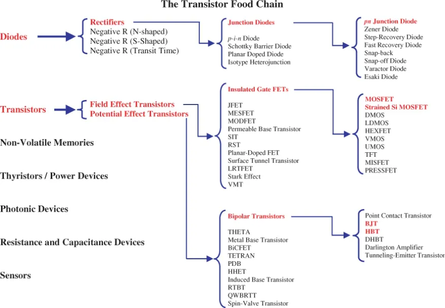
Interestingly, there are actually seven major families of semiconductor devices (only one of which includes transistors!), 74 basic classes of devices within those seven families, and another 130 derivative types of devices from those 74 basic classes (Figure 1.1) [4]. Here we focus only on three basic devices: (1) the pn homojunction junction diode (or pn junction or diode), (2) the homojunction bipolar junction transistor (or BJT), and (3) the special variant of the BJT called the silicon-germanium heterojunction bipolar transistor (or SiGe HBT). As we will see, diodes are useful in their own right, but also are the functional building block of all transistors.
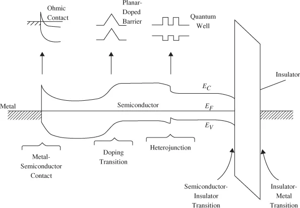
Surprisingly, all semiconductor devices can be built from a remarkably small set of materials building blocks (Figure 1.2), including [4]:
- the metal–semiconductor interface (e.g., Pt/Si; a “Schottky barrier”)
- the doping transition (e.g., a Si p-type to n-type doping transition; the pn junction)
- the heterojunction (e.g., n-AlGaAs/p-GaAs)
- the semiconductor/insulator interface (e.g., Si/SiO2)
- the insulator/metal interface (e.g., SiO2/Al).
Click here to view the historic timeline
Naming of the Transistor
The name “transistor” was actually coined by J.R. Pierce of Bell Labs, following an office betting pool which he won. He started with a literal description of what the device actually does electronically, a “transresistance amplifier,” which he first shortened to “trans-resistor,” and then finally “transistor” [3].
Why do we actually need transistors in the first place? Basically, because nature attenuates all electrical signals. By this we mean that the magnitude of all electrical signals (think “1s” and “0s” inside a computer, or an EM radio signal from a cell phone) necessarily decreases as it moves from point A to point B, something we call “loss”. When we present an (attenuated) input signal to the transistor, the transistor is capable of creating an output signal of larger magnitude (i.e., “gain”), and hence the transistor serves as a “gain block” to “regenerate” (recover) the attenuated signal in question, an essential concept for electronics. In the electronics world, when the transistor is used as a source of signal gain, we refer to it as an “amplifier.” Amplifiers are ubiquitous to all electronic systems.
Click here to view the historic timeline
Not only can the transistor serve as a wonderful nanoscale sized amplifier, but importantly it can also be used as a tiny “regenerative switch”; meaning, an on/off switch that does NOT have loss associated with it. Why is this so important? Well, imagine that the computational path through a microprocessor requires 1 000 000 binary switches (think light switch on the wall – on/off, on/off) to implement the complex digital binary logic of a given computation. If each of those switches even contributes a tiny amount of loss (which it inevitably will), multiplying that tiny loss by 1 000 000 adds up to unacceptably large system loss. That is, if we push a logical “1” or “0” in, it rapidly will get so small during the computation that it gets lost in the background noise. If, however, we implement our binary switches with gain-enabled transistors, then each switch is effectively regenerative, and we can now propagate the signals through the millions of requisite logic gates without excessive loss, maintaining their magnitude above the background noise level.
In short, the transistor can serve in one of two fundamental capacities: (1) an amplifier or (2) a regenerative switch. Amplifiers and regenerative switches work well only because the transistor has the ability to produce gain. So a logical question becomes, where does transistor gain come from? To answer this, first we need to understand pn junctions.
1.2 The pn Junction and its Electronic Applications
Virtually all semiconductor devices (both electronic and photonic) rely on pn junctions (a.k.a., “diodes”, a name which harkens back to a vacuum tube legacy) for their functionality. The simplest embodiment of a pn junction is the pn “homojunction”, meaning that within a single piece of semiconductor (e.g., silicon – Si) we have a transition between p-type doping and n-type doping (e.g., p-Si/n-Si). The opposite would be a pn heterojunction, in which the p-type doping is within one type of semiconductor (e.g., p-GaAs), and the n-type doping is within another type of semiconductor (e.g., n-AlGaAs).
Click here to view the historic timeline
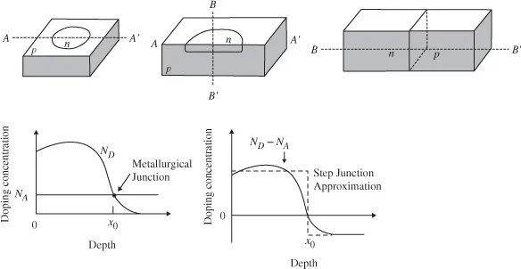
As shown in Figure 1.3, to build a pn junction we might, for instance, ion implant and then diffuse n-type doping into a p-type wafer. The important thing is the resultant “doping profile” as one moves through the junction (ND(x) – NA(x), which is just the net doping concentration). At some point in the doping transition, ND = NA, and we thus have a transition between net n-type and net p-type doping. This point is called the “metallurgical junction” (x0 in Figure 1.3) and all of the important electrical action of the junction is centered here. To make the physics easier, two simplifications are typically made: (1) Let us assume a “step junction” approximation to the real pn junction doping profile, which is just what it says, an abrupt change (a step) in doping occurring at the metallurgical junction (Figure 1.3). (2) Let us assume that all of the dopant impurities are ionized (one donor atom equals one electron, etc., an excellent approximation for common dopants in silicon at 300 K).
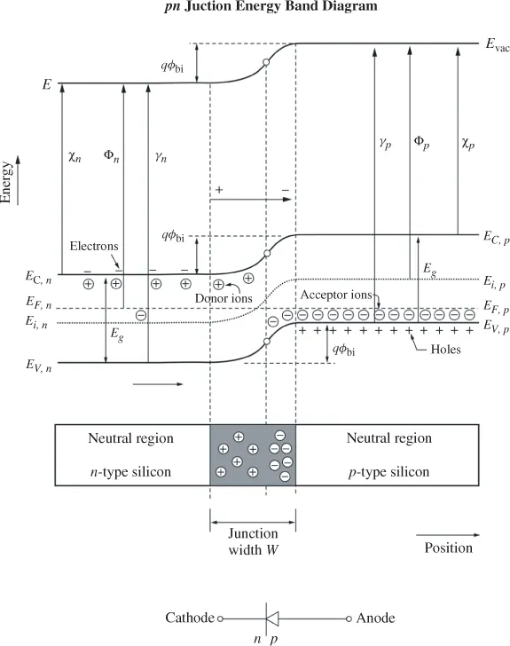
So, how does a pn junction actually work? The operation of ALL semiconductor devices is best understood at an intuitive level by considering the energy band diagram, which plots electron and hole energy as a function of position as we move physically through a device. An n-type semiconductor is electron rich (i.e., majority carriers), and hole poor (i.e., minority carriers). Conversely, a p-type semiconductor is hole-rich and electron-poor. If we imagine bringing an n-type and p-type semiconductor into “intimate electrical contact” where they can freely exchange electrons and/or holes from n to p and p to n, the final equilibrium band diagram shown in Figure 1.4 will result. Note, that under equilibrium conditions, there is no NET current flow across the junction.
Click here to view the historic timeline
We might logically wonder what actually happened inside the junction to establish this equilibrium condition. When brought into contact, the n-type side of the junction is electron rich, while the p-type side is electron poor. That is, there is a large driving force for electrons to diffuse from the n region to the p region. Recall, that there are in fact two ways to move charge in a semiconductor: (1) drift, whose driving force is the electric field (voltage/length), and (2) diffusion, whose driving force is the carrier density gradient (change in carrier density per unit distance). The latter process is what is operative here. Once in electrical contact an electron moves from the n-side to the p-side, leaving behind a positively charged donor impurity (ND+). Note, that far away from the junction, for each charged donor impurity there is a matching donated electron, hence the semiconductor is charge neutral. Once the electron leaves the n-side, however, there is no balancing charge, and a region of “space charge” results. The same thing happens on the p-side. Hole moves from p to n, leaving behind an uncompe...