2D Materials for Infrared and Terahertz Detectors provides an overview of the performance of emerging detector materials, while also offering, for the first time, a comparison with traditional materials used in the fabrication of infrared and terahertz detectors.
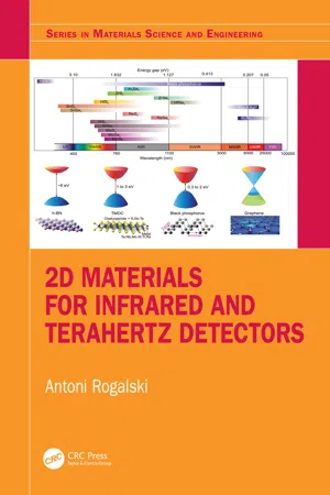
Since the discovery of graphene, its applications to electronic and optoelectronic devices have been intensively researched. The extraordinary electronic and optical properties allow graphene and other 2D materials to be promising candidates for infrared (IR) and terahertz (THz) photodetectors, and yet it appears that the development of new detectors using these materials is still secondary to those using traditional materials.
This book explores this phenomenon, as well as the advantages and disadvantages of using 2D materials. Special attention is directed toward the identification of the most-effective hybrid 2D materials in infrared and terahertz detectors, as well as future trends. Written by one of the world's leading researchers in the field of IR optoelectronics, this book will be a must-read for researchers and graduate students in photodetectors and related fields.
Features
• Offers a comprehensive overview of the different types of 2D materials used in fabrication of IR and THz detectors, and includes their advantages/disadvantages
• The first book to compare new detectors to a wide family of common, commercially available detectors that use traditional materials.
Häufig gestellte Fragen
Wie kann ich mein Abo kündigen?
Gehe einfach zum Kontobereich in den Einstellungen und klicke auf „Abo kündigen“ – ganz einfach. Nachdem du gekündigt hast, bleibt deine Mitgliedschaft für den verbleibenden Abozeitraum, den du bereits bezahlt hast, aktiv. Mehr Informationen hier.
(Wie) Kann ich Bücher herunterladen?
Derzeit stehen all unsere auf Mobilgeräte reagierenden ePub-Bücher zum Download über die App zur Verfügung. Die meisten unserer PDFs stehen ebenfalls zum Download bereit; wir arbeiten daran, auch die übrigen PDFs zum Download anzubieten, bei denen dies aktuell noch nicht möglich ist. Weitere Informationen hier.
Welcher Unterschied besteht bei den Preisen zwischen den Aboplänen?
Mit beiden Aboplänen erhältst du vollen Zugang zur Bibliothek und allen Funktionen von Perlego. Die einzigen Unterschiede bestehen im Preis und dem Abozeitraum: Mit dem Jahresabo sparst du auf 12 Monate gerechnet im Vergleich zum Monatsabo rund 30 %.
Was ist Perlego?
Wir sind ein Online-Abodienst für Lehrbücher, bei dem du für weniger als den Preis eines einzelnen Buches pro Monat Zugang zu einer ganzen Online-Bibliothek erhältst. Mit über 1 Million Büchern zu über 1.000 verschiedenen Themen haben wir bestimmt alles, was du brauchst! Weitere Informationen hier.
Unterstützt Perlego Text-zu-Sprache?
Achte auf das Symbol zum Vorlesen in deinem nächsten Buch, um zu sehen, ob du es dir auch anhören kannst. Bei diesem Tool wird dir Text laut vorgelesen, wobei der Text beim Vorlesen auch grafisch hervorgehoben wird. Du kannst das Vorlesen jederzeit anhalten, beschleunigen und verlangsamen. Weitere Informationen hier.
Ist 2D Materials for Infrared and Terahertz Detectors als Online-PDF/ePub verfügbar?
Ja, du hast Zugang zu 2D Materials for Infrared and Terahertz Detectors von Antoni Rogalski im PDF- und/oder ePub-Format sowie zu anderen beliebten Büchern aus Scienze fisiche & Fisica. Aus unserem Katalog stehen dir über 1 Million Bücher zur Verfügung.
INFRARED (IR) radiation itself was unknown until 220 years ago, when Herschel’s experiment with the thermometer was first reported. The first detector consisted of a liquid in a glass thermometer with a specially blackened bulb, to absorb radiation. Herschel built a crude monochromator that used a thermometer as a detector, so that he could measure the distribution of energy in sunlight [1].
The early history of IR was reviewed about 60 years ago in two well-known monographs [2, 3]. Much historical information can be also found in more recently published papers [4, 5]. The initial infrared detectors were based on the class of thermal detectors: thermometers, thermocouples, and bolometers [6]. In 1821, T.J. Seebeck discovered the thermoelectric effect, and soon afterward, in 1829, L. Nobili created the first thermocouple. In 1833, M. Melloni modified the thermocouple and used bismuth and antimony for its design [7]. Then, in 1835, Nobili, together with Melloni, constructed a thermopile capable of sensing a person 10 m away. The third type of thermal detector, the bolometer/thermistor, was invented by S.P. Langley in 1878. By 1900, his bolometer was 400 times more sensitive than his first efforts, and his latest bolometer could detect the heat from a cow at a distance of ¼ mile [8].
The photoconductive effect was discovered by W. Smith in 1873, when he experimented with selenium as an insulator for submarine cables [9]. This discovery provided a fertile field of investigation for several decades, though most of the effort was of doubtful quality. By 1927, over 1500 articles and 100 patents had been published on photosensitive selenium [10]. Work on the IR photovoltaic effect in naturally occurring lead sulfide, or galena, was first published by Bose in 1904 [11]; however, the IR photovoltaic effect was not exploited in a radiation detector for several more decades.
The photon detectors were developed in the twentieth century. The first IR photoconductor was developed by T.W. Case in 1917 [12]. He discovered that a substance composed of thallium and sulfur exhibited photoconductivity. Later, he found that the addition of oxygen greatly enhanced the response [13]. However, the instability of the resistance in the presence of light or polarizing voltage, the loss of responsivity due to overexposure to light or high noise, its sluggish response, and the lack of reproducibility seemed to be inherent weaknesses.
Since about 1930, the development of IR technology has been dominated by photon detectors. In about 1930, the appearance of the Cs-O-Ag phototube, with more stable characteristics, discouraged further development of photoconductive cells to a great extent until about 1940. At that time, interest in improved detectors had begun [14, 15]. In 1933, Kutzscher, at the University of Berlin, discovered that lead sulfide (from natural galena found in Sardinia) was photoconductive and had a response to about 3 μm. This work was, of course, carried out under great secrecy and the results were not generally known until after 1945. Lead sulfide was the first practical IR detector deployed in a variety of applications during the war. In 1941, Cashman improved the technology of thallous sulfide detectors, which led to successful production [16]. After success with thallous sulfide detectors, Cashman concentrated his efforts on lead sulfide and, after World War II, found that other semiconductors of the lead salt family (PbSe and PbTe) showed promise as IR detectors [17]. Lead sulfide photoconductors were brought to the manufacturing stage of development in Germany in about 1943. They were first produced in the United States at Northwestern University, Evanston, Illinois in 1944 and, in 1945, at the Admiralty Research Laboratory in England [17].
Many materials have been investigated in the IR field. Observing a history of the development of the IR detector technology, a simple theorem, after Norton [18], can be stated: “All physical phenomena in the range of about 0.1–1 eV can be proposed for IR detectors.” Among these effects are: thermoelectric power (thermocouples), change in electrical conductivity (bolometers), gas expansion (the Golay cell), pyroelectricity (pyroelectric detectors), photon drag, the Josephson effect (Josephson junctions, SQUIDs), internal emission (PtSi Schottky barriers), fundamental absorption (intrinsic photodetectors), impurity absorption (extrinsic photodetectors), low-dimensional solids [superlattice (SL), quantum well (QW), and quantum dot (QD) detectors], different types of phase transitions, and so on.
Figure 1.1 gives approximate dates for significant developments for the materials mentioned. The years during World War II saw the origins of modern IR detector technology, supported by the discovery of the transistor in 1947 by W. Shockley, J. Bardeen, and W. Brattain [19]. Recent success in applying IR technology to remote sensing problems has been made possible by the successful development of high-performance IR detectors over the past seven decades. Photon IR technology, combined with semiconductor material science, photolithography technology developed for integrated circuits, and the impetus of Cold War military preparedness, propelled extraordinary advances in IR capabilities within a short period of time during the past century [20].
FIGURE 1.1 The history of the development of IR detectors and systems. For principal military and civilian applications, four generation systems can be considered: first-generation (scanning systems), second-generation (staring systems, electronically scanned), third-generation (staring systems, with large number of pixels and two-color functionality), and fourth-generation (staring systems with very large number of pixels, multi-color functionality, 3D ROIC, and other on-chip functions) systems, offering other functions, e.g. better radiation/pixel coupling, avalanche multiplication in pixels, and polarization/phase sensitivity.
1.1 Historical Aspects of Modern Infrared Technology
During the 1950s, IR detectors were built using single-element-cooled lead salt detectors, primarily for anti-air missile seekers. Usually, lead salt detectors were polycrystalline and were produced by vacuum evaporation and chemical deposition from a solution, followed by a post-growth sensitization process [17]. The preparation process of lead salt photoconductive detectors was usually not well understood, and reproducibility could be achieved only after following well-tried recipes. The first extrinsic photoconductive detectors were reported in the early 1950s [21], after the discovery of the transistor, which stimulated a considerable improvement in the growth and material purification techniques. Since the techniques for controlled introduction of impurities became available for germanium earlier, the first high-performance extrinsic detectors were based on germanium. Extrinsic, photoconductive response from copper, zinc, and gold impurity levels in germanium gave rise to devices using the 8- to 14-μm longwave IR (LWIR) spectral window and beyond to the 14- to 30-μm very longwave IR (VLWIR) region. The extrinsic photoconductors were widely used at wavelengths beyond 10 μm, prior to the development of the intrinsic detectors. They must be operated at lower temperatures to achieve performance similar to that of intrinsic detectors, and a sacrifice in quantum efficiency is required to avoid thick detectors.
In 1967, the first comprehensive extrinsic Si detector-oriented paper was published, by Soref [22]. However, the state of the extrinsic Si was not changed significantly. Although Si has several advantages over Ge (namely, a lower dielectric constant, giving shorter dielectric relaxation times and lower capacitance, higher dopant solubility, a larger photoionization cross section for greater quantum efficiency, and a lower refractive index for lower reflectance), these were not sufficient to warrant the necessary development efforts needed to bring it to the level of the by-then highly developed Ge detectors. After the concept lay dormant for about 10 years, extrinsic Si was reconsidered after the invention of charge-coupled devices (CCDs) by Boyle and Smith [23]. In 1973, Shepherd and Yang [24] proposed the metal-silicide/silicon Schottky barrier detectors. For the first time, it became possible to have much more sophisticated readout schemes, so that both detection and readout could be implemented in one common silicon chip.
At the same time, rapid advances were being made in narrow-bandgap semiconductors, that would later prove useful in extending wavelength capabilities and improving sensitivity. The first such material was InSb, a member of the newly discovered III-V compound semiconductor family. The interest in InSb stemmed, not only from its small energy gap, but also from the fact that it could be prepared in single crystal form, using a conventional technique. The end of the 1950s and the beginning of the 1960s saw the introduction of narrow-gap semiconductor alloys in III–V (InAs1–xSbx), IV–VI (Pb1–xSnxTe), and II–VI (Hg1–xCdxTe) material systems. These alloys allowed the bandgap of the semiconductor, and hence the spectral response of the detector, to be custom tailored for specific applications. In 1959, research by Lawson and coworkers [25] triggered the development of variable-bandgap Hg1–xCdxTe (H...