
eBook - ePub
Low Temperature Chemical Nanofabrication
Recent Progress, Challenges and Emerging Technologies
Omer Nur, Magnus Willander
This is a test
Buch teilen
- 252 Seiten
- English
- ePUB (handyfreundlich)
- Über iOS und Android verfügbar
eBook - ePub
Low Temperature Chemical Nanofabrication
Recent Progress, Challenges and Emerging Technologies
Omer Nur, Magnus Willander
Angaben zum Buch
Buchvorschau
Inhaltsverzeichnis
Quellenangaben
Über dieses Buch
Low Temperature Chemical Nanofabrication: Recent Progress, Challenges and Emerging Technologies offers a thorough and theoretical background to nanoscale fabrication phenomena, also covering important practical applications. It covers the conventional top down and the newly emerging bottom up processing methods. The latter has proven to be feasible for obtaining device quality material and can either be performed using high or low temperature processing. Low temperature (?100 oC), in particular, is becoming increasingly used due to its simplicity and varied applications, with huge benefits for developing new devices and flexible non-conventional substrates.
This important resource is ideal for researchers seeking to learn more about the fundamental theories related to nanoscale phenomena and nanofabrication.
- Provides extensive coverage of nanofabrication techniques, allowing researchers to learn different nanofabrication techniques
- Explores different applications for low-temperature chemical nanofabrication
- Cogently explains how low-temperature chemical nanofabrication differs from other nanofabrication techniques, assessing the pros and cons of each
Häufig gestellte Fragen
Wie kann ich mein Abo kündigen?
Gehe einfach zum Kontobereich in den Einstellungen und klicke auf „Abo kündigen“ – ganz einfach. Nachdem du gekündigt hast, bleibt deine Mitgliedschaft für den verbleibenden Abozeitraum, den du bereits bezahlt hast, aktiv. Mehr Informationen hier.
(Wie) Kann ich Bücher herunterladen?
Derzeit stehen all unsere auf Mobilgeräte reagierenden ePub-Bücher zum Download über die App zur Verfügung. Die meisten unserer PDFs stehen ebenfalls zum Download bereit; wir arbeiten daran, auch die übrigen PDFs zum Download anzubieten, bei denen dies aktuell noch nicht möglich ist. Weitere Informationen hier.
Welcher Unterschied besteht bei den Preisen zwischen den Aboplänen?
Mit beiden Aboplänen erhältst du vollen Zugang zur Bibliothek und allen Funktionen von Perlego. Die einzigen Unterschiede bestehen im Preis und dem Abozeitraum: Mit dem Jahresabo sparst du auf 12 Monate gerechnet im Vergleich zum Monatsabo rund 30 %.
Was ist Perlego?
Wir sind ein Online-Abodienst für Lehrbücher, bei dem du für weniger als den Preis eines einzelnen Buches pro Monat Zugang zu einer ganzen Online-Bibliothek erhältst. Mit über 1 Million Büchern zu über 1.000 verschiedenen Themen haben wir bestimmt alles, was du brauchst! Weitere Informationen hier.
Unterstützt Perlego Text-zu-Sprache?
Achte auf das Symbol zum Vorlesen in deinem nächsten Buch, um zu sehen, ob du es dir auch anhören kannst. Bei diesem Tool wird dir Text laut vorgelesen, wobei der Text beim Vorlesen auch grafisch hervorgehoben wird. Du kannst das Vorlesen jederzeit anhalten, beschleunigen und verlangsamen. Weitere Informationen hier.
Ist Low Temperature Chemical Nanofabrication als Online-PDF/ePub verfügbar?
Ja, du hast Zugang zu Low Temperature Chemical Nanofabrication von Omer Nur, Magnus Willander im PDF- und/oder ePub-Format sowie zu anderen beliebten Büchern aus Tecnologia e ingegneria & Scienza dei materiali. Aus unserem Katalog stehen dir über 1 Million Bücher zur Verfügung.
Information
Chapter 1
Introduction
Abstract
In this chapter some of the very early findings related to nanoscale objects will be discussed. Then the accidental early work from the 1940s related to nanofabrication is reviewed. Then other important historical findings related to nanofabrication are stated. This will be followed by a discussion on the driving force that led to the rise of today’s era of modern nanotechnology.
Keywords
Early finding of nanoscale phenomenon; nanotechnology driving force; what is special about nanoscale objects
1.1 When nanotechnology started?
Although the word “nano” is originally derived from the Greek word “nânos” meaning a dwarf, the term nanotechnology, which combines the two words nano and technology, was first introduced in 1974 by the Japanese scientist Norio Taniguchi of Tokyo Science University [1]. However, about 15 years before that, specifically in December 1959, the Nobel laureate physicist Richard Feynman described nanotechnology, although not using the term nanotechnology, during a famous popular speech, “There is Plenty of Room at the Bottom,” at the annual meeting of the American Physical Society at Caltech, CA, USA. Feynman had looked two decades ahead and had envisioned and described the possible potential of manipulating and controlling matter on a relatively small scale [2]. Specifically Feynman said: “I would like to describe a field in which little has been done but in which an enormous amount can be done in principle. The field is not quite the same as the others in that it will not tell us much of fundamental physics (in the sense of ‘what are the strange particles?’); but it is more like solid-state physics in the sense that it might tell us much of great interest about the strange phenomena that occur in complex situations. Furthermore, a point that is most important is that it would have an enormous number of technical applications. What I want to talk about is the problem of manipulating and controlling things on a small scale” [2]. At the time when Feynman presented his popular visionary talk, there were no spectroscopy tools that could enable scientists to easily visualize, control, or manipulate matter at a relatively small scale. It was more than two decades after Feynman’s suggestion of the new area of physics, that scientists were able to visualize with high-precision and control/manipulate atoms and clusters. This was due to the development of the scanning tunneling microscope by IBM scientists in the 1980s, which allowed high-precision visualization at scales of the order of the chemical bond length. These experimental analytical tool developments, combined with advances in theory, and the modeling of matter, has allowed the potential of nanotechnology to be seen and its utilization to be within the reach of human capability.
Nevertheless, long before this, particularly in the early 1940s, some research efforts, while working blindly with no imaging/visualization techniques available, performed the characterization of nanomaterials [3]. In 1944 a paper was published where Fuller characterized nanoscale zinc oxide material using stereoscopic electron microscopy combined with the graphical method of crystallographic stereographic projection [3]. In this pioneering (and long and tedious) work, Fuller came to the conclusion that the structure he was studying was in fact named a “fourlings structure” of a few nanometers in size. The fourlings structure of zinc oxide is a structure with a four-leg arrangement in such a way that the plane formed by each pair of legs is perpendicular to the other plane formed by the second pair of the four legs. The reader of this published work will no doubt see the amount of effort required for Fuller to come to his conclusion. In fact such a conclusion can today be reached within a maximum of 15 minutes of investigation using modern imaging spectroscopy methods, like high-resolution scanning electron microscopy, etc.
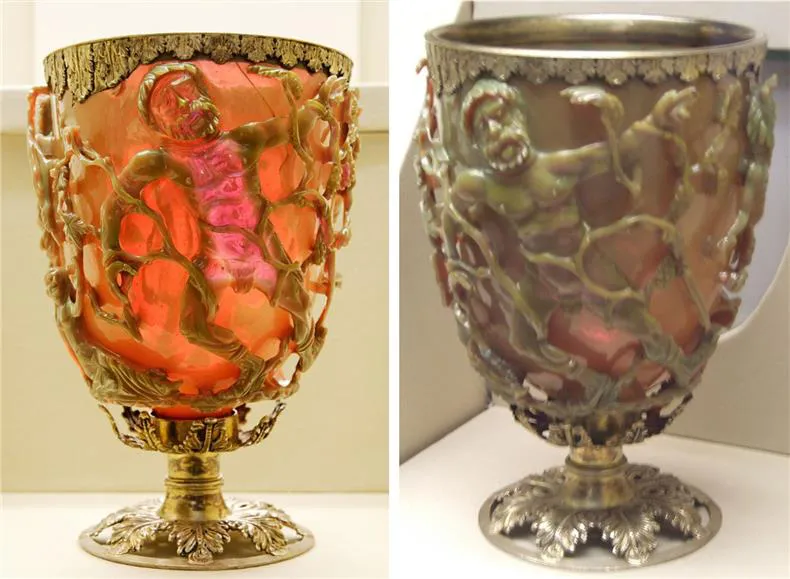
The mystery of the change of color of a 1600-year-old Roman goblet cup has amazed scientists for centuries and was not resolved until 1990. As seen in Fig. 1.1, the mysterious Lycurgus Cup, which is made of pigmented glass and decorated with metallic rings, changes color as light is shone on it. It also shows a different color depending on the direction from which the person views it. After being thoroughly investigated, scientists came to the conclusion that the pigmentation is actually made of silver and gold nanoparticles (NPs) of sizes down to 50 nm. This mysterious chalice which is displayed at the British Museum, London, was fabricated using a technique similar to what we use today in nanotechnology. The change of color is explained by the vibration of metallic NPs as light falls on them—more details about why nanosized silver and gold have his ambiguous behavior will be explained in Chapter 2, Phenomenon at the nanoscale. The Lycurgus chalice which is indeed an “out-of-place artifact” (OOPArt) has led scientists to consider the Romans as the pioneers of nanotechnology. But does the search end here? The answer is no!.
Other much older findings discovered only recently have suggested that nanomatter might have been processed and fabricated by humans long before the Romans [4]. In 1991 different morphological nanostructures, e.g., spirals, coils, and shafts, dating back to about 300,000 years, were found near the banks of Russia’s Kozhim, Narada, and Balbanyu rivers. These findings were discovered at depths between 10 and 40 feet, and their geological stratus indicated that they are between 20,000 and 318,000 years old. There has been an argument that suggested that these tiny objects might have been left from test rockets experiments from a nearby space research station. Nevertheless, reports have proved that these tiny objects are too old to have originated from modern manufacturing at the claimed space station. Further it was also proved that these thousands of years’ old tiny nanostructures are of technological origin. In 1996 Dr. E.W. Matvejeva from the Central Scientific Research Department of Geology and Exploitation of Precious Metals in Moscow wrote that, despite being thousands of years old, the components are of a technological origin. Although this discovery has raised a debate which continues today, it suggests that an advanced culture with high technological capabilities might have existed during the ancient Pleistocene era [4]. There are also claims that these tiny nanostructures, which were fabricated using an advanced technology, do in fact originate from extraterrestrial creatures who gave them to humans or they may have been discarded by extraterrestrials. This claim has been stated with no proof apart from the fact that there was no explanation for the existence of such old technologically advanced metal nanostructures.
However we can ask the following question: is the findings of the OOPArts 300,000 years back is the oldest discovered nanomaterials? The answer is definitely no! According to findings using modern spectroscopy imaging and characterization tools, nanomaterials and nanostructures existed long before that, actually since antiquity. Now humans have learned that nature has always been capable of assembling and creating self-assembled nanostructures and is adapted to nanoengineering [5]. This implies that nature has been assembling nanostructures from time immemorial. To mention some examples, let us consider the structure and functionality of some natural old existing nanomaterials. Let us consider the structure and functionality of allophane and smectite which are nanomaterials of geological and pedological origin [5].
The allophane structure (see Fig. 1.2) [6] is composed of a hydrous aluminosilicate group appearing as an irregular hollow spherical NP. The outer diameter of the allophane is 3.5–5.0 nm, while the wall thickness is of the range 0.7–1.0 nm [8,9]. The allophane as a nanospherical morphology is a pH-dependent clay mineral that has unique characteristics; it carries both negative and positive charge separated by location in the nanosphere [7]. The positive charge is originating from the aluminol group located at the pore region of the nanosphere, while the negative charge originates from the silanol group located at the inner side of the allophane nanosphere. Smectite has a unit particle composed of an aluminosilicate layer with sizes ranging from few tenths of a nanometer to a few hundreds of nanometers, width and length, respectively. The thickness of the layer is about 1 nm only [8]. Due to the relatively small size of both allophane and smectite, their specific surface area is relatively quite large (about 700–900 m2/g); this implies that a teaspoon of allophane will probably have a surface area much larger than a football playing field [8]. The relatively small size and huge surface area of these naturally occurring materials, that is, allophane and smectite, along with their peculiar charge characteristics enable them to be excellent contamination sorbent materials and they are widely employed in industrial applications to remove pollutants. Beside the use of natural occurring allophane NPs in industrial application, they have found their way into medical applications, for example, cytotoxicity of lung cancer [10]. Such old naturally occurring nanostructures have in fact become a source of inspiration for humans to artificially engineer many fascinating new prototypes and useful nanomorphologies of different materials [11]. Another important example of natural occurring nanomaterials is the existence of NPs in natural fresh drinking water [12]. It is now very well established that during evolution living organisms have been shown to be capable of designing biomolecules through self-assembly, building up very smart and complicated organized systems [11]. Hence it is acceptable to say that the existence of nanomaterials is as old as the universe. It is only our relatively recent ability to see, manipulate, and use nanomaterials that has led to the emergence and the early maturity of this fascinating branch of science only recently, that is, during the 21st century. It also worth mentioning that most of the, although not all, naturally occurring nanostructures found today have been evolved at relatively low temperatures (<100°C) and as free-standing structures, i.e., no need for a substrate or stand to be utilized to fabricate nanostructures.
