![]()
Chapter 1
Overview
This chapter is essentially the same as Chapter 1 from Part A. Related video lecture available at course website, Scientific Overview.
“Everyone” has a smartphone these days, and each smartphone has more than a billion transistors, making transistors more numerous than anything else we could think of. Even the proverbial ants, I am told, have been vastly outnumbered.
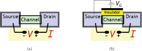
There are many types of transistors, but the most common one in use today is the Field Effect Transistor (FET), which is essentially a resistor consisting of a “channel” with two large contacts called the “source” and the “drain” (Fig. 1.1a).
Fig. 1.1 (a) The Field Effect Transistor (FET) is essentially a resistor consisting of a channel with two large contacts called the source and the drain across which we attach the two terminals of a battery. (b) The resistance R = V/I can be changed by several orders of magnitude through the gate voltage VG.
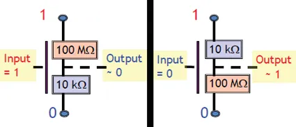
The resistance (R) = Voltage (V)/Current (I) can be switched by several orders of magnitude through the voltage VG applied to a third terminal called the “gate” (Fig. 1.1b) typically from an “OFF” state of ∼ 100 MΩ to an “ON” state of ∼ 10 kΩ. Actually, the microelectronics industry uses a complementary pair of transistors such that when one changes from 100 MΩ to 10 kΩ, the other changes from 10 kΩ to 100 MΩ. Together they form an inverter whose output is the “inverse” of the input: a low input voltage creates a high output voltage while a high input voltage creates a low output voltage as shown in Fig. 1.2.
A billion such switches switching at GHz speeds (that is, once every nanosecond) enable a computer to perform all the amazing feats that we have come to take for granted. Twenty years ago computers were far less powerful, because there were “only” a million of them, switching at a slower rate as well.
Fig. 1.2 A complementary pair of FET’s form an inverter switch.
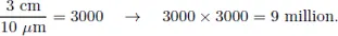
Both the increasing number and the speed of transistors are consequences of their ever-shrinking size and it is this continuing miniaturization that has driven the industry from the first four-function calculators of the 1970s to the modern laptops. For example, if each transistor takes up a space of say 10 µm × 10 µm, then we could fit 9 million of them into a chip of size 3 cm × 3 cm, since
That is where things stood back in the ancient 1990s. But now that a transistor takes up an area of ∼ 1 µm × 1 µm, we can fit 900 million (nearly a billion) of them into the same 3 cm × 3 cm chip. Where things will go from here remains unclear, since there are major roadblocks to continued miniaturization, the most obvious of which is the difficulty of dissipating the heat that is generated. Any laptop user knows how hot it gets when it is working hard, and it seems difficult to increase the number of switches or their speed too much further.
This book, however, is not about the amazing feats of microelectronics or where the field might be headed. It is about a less-appreciated by-product of the microelectronics revolution, namely the deeper understanding of current flow, energy exchange and device operation that it has enabled, which has inspired the perspective described in this book. Let me explain what we mean.
1.1Conductance
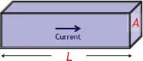
A basic property of a conductor is its resistance R which is related to the cross-sectional area A and the length L by the relation
The resistivity ρ is a geometry-independent property of the material that the channel is made of. The reciprocal of the resistance is the conductance G which is written in terms of the reciprocal of the resistivity called the conductivity σ. So what determines the conductivity?
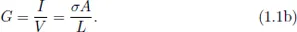
Our usual understanding is based on the view of electronic motion through a solid as “diffusive” which means that the electron takes a random walk from the source to the drain, traveling in one direction for some length of time before getting scattered into some random direction as sketched in Fig. 1.3. The mean free path, that an electron travels before getting scattered is typically less than a micrometer (also called a micron = 10−3 mm, denoted µm) in common semiconductors, but it varies widely with temperature and from one material to another.
Fig. 1.3 The length of the channel of an FET has progressively shrunk with every new generation of devices (“Moore’s law”) and stands today at 14 nm, which amounts to ∼ 100 atoms.
It seems reasonable to ask what would happen if a resistor is shorter than a mean free path so that an electron travels ballistically (“like a bullet”) through the channel. Would the resistance still be proportional to length as described by Eq. (1.1a)? Would it even make sense to talk about its resistance?
These questions have intrigued scientists for a long time, but even twenty five years ago one could only speculate about the answers. Today the answers are quite clear and experimentally well established. Even the transistors in commercial laptops now have channel lengths L ∼ 14 nm, corresponding to a few hundred atoms in length! And in research laboratories people have even measured the resistance of a hydrogen molecule.
1.2Ballistic Conductance
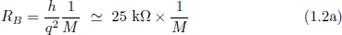
It is now clearly established that the resistance RB and the conductance GB of a ballistic conductor can be written in the form
where q, h are fundamental constants and M represents the number of effective channels available for conduction. Note that we are now using the word “channel” not to denote the physical channel in Fig. 1.3, but in the sense of parallel paths whose meaning will be clarified in the first two parts of this book. In future we will refer to M as the number of “modes”, a concept that is arguably one of the most important lessons of nanoelectronics and mesoscopic physics.
1.3What Determines the Resistance?
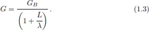
The ballistic conductance GB (Eq. (1.2b)) is now fairly well-known, but the common belief is that it is relevant only for short conductors and belongs in a course on special topics like mesoscopic physics or nanoelectronics. We argue that the resistance for both long and short conductors can be written in terms of GB (λ: mean free path)
Ballistic and diffusive conductors are not two different worlds, but rather a continuum as the length
L is increased. For
Eq. (
1.3) reduces to
while for
which morphs into Ohm’s law (Eq. (1.1b)) if we write the conductivity as
The conductivity of long diffusive conductors is determined by the number of modes per unit area (M/A) which represents a basic material property that is reflected in the conductance of ballistic conductors.
By contrast, the standard expressions for conductivity are all based on bulk material properties. For example freshman physics texts typically describe the Drude formula (momentum relaxation time: τm):
involving the effective mass (
m) and the density of free electrons (
n). This is the equation that many researchers carry in their head and use to interpret experimental data. However, it is tricky to apply if the electron dynamics
is not described by a simple positive effective mass
m. A more general but less well-known expression for the conductivity involves the density of states (
D) and the diffusion coefficient
In Part A of this book we used fairly elementary arguments to establish the new formula for conductivity given by Eq. (1.4) and show its equivalence to Eq. (1.6). In Part A we also introduced an energy band model and related Eqs. (1.4) and (1.6) to the Drude formula (Eq. (1.5)) under the appropriate conditions when an effective mass can be defined.
We could combine Eqs. (1.3) and (1.4) to say that the standard Ohm’s law (Eqs. (1.1)) should be replaced by the res...