![]()
Chapter 1
Size Matters: Optical Properties of Nanoparticles
Christian von Borczyskowskia and Eduard Zenkevichb
a Institute of Physics, Center for Nanostructured Materials and Analytics, Technische Universität Chemnitz, Reichenhainer Str. 70, D-09107 Chemnitz, Germany
b Department of Information Technologies and Robototechnique, National Technical University of Belarus, Prospect Nezavisimosti 65, 220013 Minsk, Belarus
One of the fascinations about nanoparticles or nanocrystals (NCs) built from a few to several thousand atoms is the fact that they are from a quantum mechanical point of view a class of materials between atoms and solids showing properties of both of them. Though a deep understanding of their properties emerged only during the last few decades, the related versatility has been used already since centuries. Probably the most obvious feature is the dependence of properties, like the color, on the size of NCs, both for semiconducting and for metal particles. A lot of features can nowadays be understood in terms of quantum confinement resembling in its most simple approximation, the “particle in a box” model taught in undergraduate courses on quantum mechanics. NCs falling into this category are thought of as 1D quantum objects and have been also named “quantum dots” (QDs). We will use this name, or QDs, throughout the book. The fundamental optical excitations in a semiconducting QD depend on electrons, holes, and excitons in a 3D (confining) potential. Systematic research began in the early 1980s with the identification of quantum confinement in small semiconductor NCs. Different from scaling down nanostructures lithographically as is the present standard in micro-and nanotechnology, QDs are in most cases formed via bottom-up approaches in glasses or polymers or from solutions. In general, semiconductor nanostructures show an amazing variety of interesting properties different from conventional solid state materials. A recent comprehensive review outlines the prospects of nanoscience with NCs [Kovalenko et al., 2015].
Though quantum confinement and its consequences already open an enormously wide field with respect to both fundamental research and applications, QDs are not only in between atoms and solids but depend to a large extent on surface properties. This can be considered not as a disadvantage but just the opposite since elementary processes such as charge accumulation or catalysis depend essentially on interface properties. In this book, we will pay special attention from an empirical point of view to surface or interface features. Especially we will discuss how they can be tuned by various means.
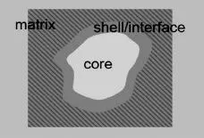
Figure 1.1 shows schematically what has to be taken into account when analyzing a QD, including influences outside the intrinsically confining potential. We have indicated that a crystal structure may not be perfect under realistic conditions. In any case a crystal structure includes facets and surface domains, depending on crystal symmetry. Besides the QD core (e.g., CdSe as a II–VI semiconductor), QDs may contain shells from other semiconductor materials (e.g., ZnS) and/or organic surfactants (ligands). The latter are essential when QDs are synthesized from solution to stop further growth or to protect from aggregation (Oswald ripening). Such a structure already constitutes two to three interfaces. In general, QDs are embedded in a matrix (liquid, polymer, glass). Moreover, in the case of thin films, a supporting substrate might also have to be taken into account. All these subsystems have to be followed since though the electronic wavefunctions are confined in a potential, they might tunnel through confining barriers, “exploring” the corresponding environment on a nanoscale. These considerations are essential, especially with respect to applications.
A whole bunch of textbooks describes the treatment of excited states of (semiconductor) QDs, taking into account quantum confinement [Woggon, 1997; Gaponenko, 1998; Gaponenko, 2010; Rogach, 2008; Gavrilenko, 2011]. Therefore we will restrict ourselves here to the basic principles without going into detail. The band energy of a particle in a quasi-infinite bulk semiconductor is described by the dispersion relation
with band-gap energy EG and the reciprocal effective mass 1/m* at k = 0 according to
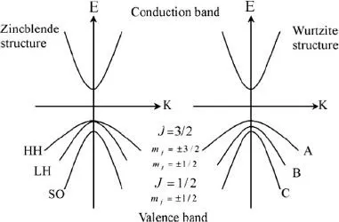
The band structure is characterized in Fig. 1.2 for II–VI semiconductors (e.g., CdSe or ZnS) with a direct band gap.
For semiconductors like CdS, CdSe, ZnS, or ZnSe, the conduction band is formed from s orbitals of the metal ions Cd or Zn, whereas the valence band corresponds to porbitals of the chalcogenides S or Se. While the conduction band can in most cases be approximated by parabolic potentials, the valence bands are partly degenerate and more complex, depending on the crystal structure (zinc-blende or wurtzite). We will describe the details after introducing quantum confinement.
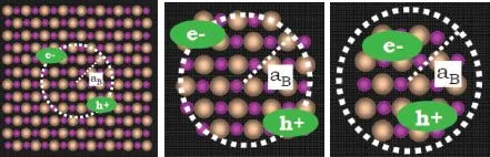
Without quantum size effects the (optically generated) electron–hole pair is a hydrogen-like bound state, the so-called exciton. The interacting hole and electron (electron-hole pair) are described by the Hamiltonian in Eq. 1.3, which applies when the size of an NC is comparable to the critical length parameters, that is, the de Broglie wavelength λ and the exciton Bohr radius aB of the quasi-particles: electron, hole, and exciton. It is described as
| (1.3) |
where is the effective mass of the electron (hole), respectively, and the static dielectric constant of the bulk semiconductor is ε2 (~9.5 for CdSe). The exciton is similarly, as a hydrogen atom, characterized by the exciton Bohr radius aB according to
| (1.4) |
aB is in the range of 1–10 nm for typical II–VI semiconductors. In this range the QD is with respect to lattice constants of a macroscopic solid, but quantum size effects become important for the quasiparticles. Figure 1.3 shows schematically how the various scales (lattice constant, Bohr radius, crystal size) are related.