
eBook - ePub
Electrostatic Discharge Protection
Advances and Applications
Juin J. Liou, Juin J. Liou
This is a test
Partager le livre
- 304 pages
- English
- ePUB (adapté aux mobiles)
- Disponible sur iOS et Android
eBook - ePub
Electrostatic Discharge Protection
Advances and Applications
Juin J. Liou, Juin J. Liou
Détails du livre
Aperçu du livre
Table des matières
Citations
À propos de ce livre
- Covers ESD concepts, design strategies, Models, and Protection Solutions in one volume
- Highlights end-user applications and environment
- Explains how integrated circuits used in consumer electronics, such as cellphone, can be protected against the ESD event
- Provides necessary information on the backgrounds, methods, and approaches for issues pertinent to the design and developments of ESD protection solutions
- Includes contributions by the top experts in the field with affiliations from US; Japan; China;Italy; and Taiwan
Foire aux questions
Comment puis-je résilier mon abonnement ?
Il vous suffit de vous rendre dans la section compte dans paramètres et de cliquer sur « Résilier l’abonnement ». C’est aussi simple que cela ! Une fois que vous aurez résilié votre abonnement, il restera actif pour le reste de la période pour laquelle vous avez payé. Découvrez-en plus ici.
Puis-je / comment puis-je télécharger des livres ?
Pour le moment, tous nos livres en format ePub adaptés aux mobiles peuvent être téléchargés via l’application. La plupart de nos PDF sont également disponibles en téléchargement et les autres seront téléchargeables très prochainement. Découvrez-en plus ici.
Quelle est la différence entre les formules tarifaires ?
Les deux abonnements vous donnent un accès complet à la bibliothèque et à toutes les fonctionnalités de Perlego. Les seules différences sont les tarifs ainsi que la période d’abonnement : avec l’abonnement annuel, vous économiserez environ 30 % par rapport à 12 mois d’abonnement mensuel.
Qu’est-ce que Perlego ?
Nous sommes un service d’abonnement à des ouvrages universitaires en ligne, où vous pouvez accéder à toute une bibliothèque pour un prix inférieur à celui d’un seul livre par mois. Avec plus d’un million de livres sur plus de 1 000 sujets, nous avons ce qu’il vous faut ! Découvrez-en plus ici.
Prenez-vous en charge la synthèse vocale ?
Recherchez le symbole Écouter sur votre prochain livre pour voir si vous pouvez l’écouter. L’outil Écouter lit le texte à haute voix pour vous, en surlignant le passage qui est en cours de lecture. Vous pouvez le mettre sur pause, l’accélérer ou le ralentir. Découvrez-en plus ici.
Est-ce que Electrostatic Discharge Protection est un PDF/ePUB en ligne ?
Oui, vous pouvez accéder à Electrostatic Discharge Protection par Juin J. Liou, Juin J. Liou en format PDF et/ou ePUB ainsi qu’à d’autres livres populaires dans Technology & Engineering et Electrical Engineering & Telecommunications. Nous disposons de plus d’un million d’ouvrages à découvrir dans notre catalogue.
Informations
1 Introduction to Electrostatic Discharge Protection
Juin J. Liou
CONTENTS
1.1 Background of Electrostatic Discharge Events
1.2 ESD Protection Design Principles
1.3 ESD Measurement and Testing
References
1.1 BACKGROUND OF ELECTROSTATIC DISCHARGE EVENTS
Electrostatic discharge (ESD) is one of the most prevalent threats to the integrity of electronic components and integrated circuits (ICs). It is an event in which a finite amount of charge is transferred from one object (i.e., human body) to another (i.e., microchip). This process can result in a very high current passing through the object within a very short period of time [1,2]. A common ESD phenomenon is shown in Figure 1.1, where a person is shocked by an ESD from the metal doorknob to the ground via the human body. In this case, the human body is the charge source, the metal knob is the ground, and the human body skin is the conducting path between the source and ground. The amount of charges on a body is typically described by the voltage, and the voltage level depends on factors such as flooring material and air humidity. When a microchip or an electronic system is subject to an ESD event, the huge ESD-induced current can damage the microchip and cause malfunction to the electronic system if the ESD-generated energy in the object cannot be dissipated quickly enough. Figure 1.2 shows various damages found in microchips resulted from ESD stresses. These damages can be summarized into three categories: oxide breakdown, junction failure, and metal fusing. It is estimated that about 35% of all damaged microchips are ESD related, resulting in a loss of revenue of several hundred million dollars in the global semiconductor industry every year [3]. The continuing scaling of complementary metal-oxide semiconductor (CMOS) technology makes ESD-induced failures even more prominent, and one can predict with certainty that the availability of effective and robust ESD protection solutions will become a critical and essential component to the advancement and commercialization of the modern and next-generation Si, GaAs, GaN, and other technologies [4–7].
In this chapter, the fundamentals of ESD, including its mechanisms, standards, protection design principles, and testing, will be briefly introduced.
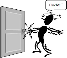
FIGURE 1.1 A commonly known ESD phenomenon.
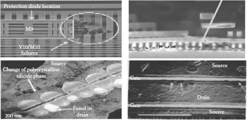
FIGURE 1.2 ESD-induced damages (clockwise, from the upper left-hand corner) associated with interconnect burnout, metal contact rupture, junction melting, and crystal structure change.
The following three processes can generate charges on an object: the triboelectrification process where the charges are generated because of the contacting and rubbing of two different objects, the inductive process where the charges are generated because of the presence of an electric field, and the conductive process where an uncharged object is charged after it is in touch with another charged object. The amount of charge generated increases with decreasing air humidity, and the severity of the charge is described by the voltage. For example, a human body can carry more than 10,000 V of ESD in a dry environment and a few hundred volts of ESD in a wet environment [8].
Various ESD events taking place in our daily life and in microchip manufacturing environment can be classified into four standards or models: the human body model (HBM), which describes an event when a charged person touches a microchip; the machine model (MM), which describes an event when a charged metal object is in contact with a microchip; the charged device model (CDM), which describes an event when a charged device is in contact with a grounded object; and the International Electrotechnical Commission (IEC), which describes an event when a charged cable/wire is in contact with an electronic component.
Some comments on the different ESD standards are in order. HBM is a mature, well-understood ESD model for simulating charge transfer from a person’s finger to an electronic component. However, recent industry data indicates that HBM rarely simulates real-world ESD failures. Latest-generation package styles such as mBGAs, SOTs, SC70s, and CSPs with mm-range dimensions are often effectively too small for people to handle with fingers. Even in cases of relatively large components, most high-volume component and board manufacturing uses automated equipment, so humans rarely touch the components. CDM can more successfully replicate in-house and customer IC failures at the component level. It simulates the damage induced when a metal pin or solder ball on a charged IC package is instantaneously discharged via contact with a metallic object at ground potential.
An effective way to protect an electronics system against ESD events is to incorporate an ESD protection structure on the microchip (called the on-chip ESD protection) to increase the survivability of the core circuit when an ESD strikes. In such a structure, all input, output, and power supply pins of the core circuit are connected to the ground bus/rail via ESD protection devices. These ESD devices must be in the off-state during the normal system operation (i.e., in the absence of an ESD event), must be turned on quickly when an ESD event takes place so that the current generated by the ESD event can be conducted by ESD protection devices and discharged to the ground, must themselves not be damaged by the ESD stress, must clamp the pins to a sufficiently low voltage during the ESD event, and must return to the off-state after the ESD event has passed [9,10].
There are a number of technologies for which this on-chip ESD protection is not feasible and using an off-chip ESD protection solution becomes necessary. The off-chip ESD protection structure can be incorporated in electrical cables, in connectors, in ceramic carriers, or on circuit boards.
In the future, designing effective ESD protection solutions will become increasingly difficult and costly. As shown in Figure 1.3, the cost for designing ESD protection solutions in general increases with CMOS technology advancement (i.e., the technology node reducing from 180 nm to 45 nm) [11]. Furthermore, using custom solutions (ESD protection solutions designed with customized and optimized approaches) has the advantage of cutting the cost over using public solutions (ESD protection solutions designed with generalized and off-the-shelf approaches). The operation of an ESD protection device is described by the black curve in Figure 1.4. It is sandwiched between the IC operating area on the left and the IC reliability constraint on the right. As the CMOS technology is advancing, this design window becomes smaller, making the ESD protection design more challenging.
1.2 ESD PROTECTION DESIGN PRINCIPLES
As mentioned in the beginning of the chapter, effective ESD protection solutions are must-haves for modern ICs. The design of ESD protection solutions, however, is challenging and difficult because of the constraints imposed by the technology, IC operation, and customer demand. In this section, we will focus on issues pertinent to the design of on-chip ESD protection solutions.
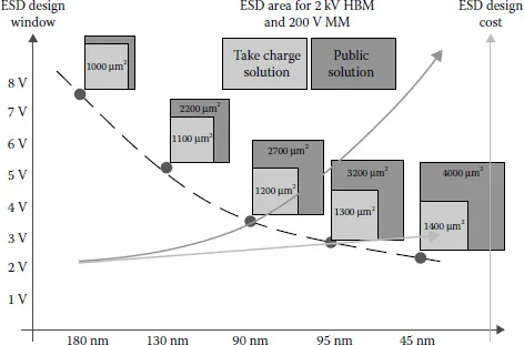
FIGURE 1.3 ESD design cost as a function of the CMOS technology using the custom solution (light gray line) and the public solution (dark gray line). (Data from Van Mele, K., Effective ESD Strategies in Nano-CMOS IC Design, Sarnoff Europe, Gistel, Belgium, http://www.chipestimate.com/techtalk.php?d=2007-12-04.)
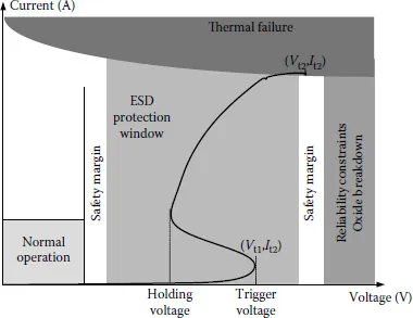
FIGURE 1.4 Illustration of IC operating area, ESD design window, I–V curve of ESD protection device, and IC reliability constraint.
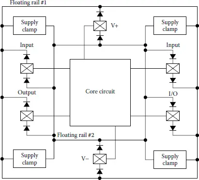
FIGURE 1.5 Typical ESD protection scheme constructed using diodes at the I/O pins and supply clamps between the power supply and ground bus.
A typical on-chip ESD protection scheme is shown in Figure 1.5, where two ESD protection devices (i.e., diodes) are connected to each input/output (I/O) pin and several ESD protection devices/circuits, called supply clamps, are connected between the power supply rail Vdd and ground bus Vss. Such a scheme is used to protect the core circuit against positive- and negative-polarity ESD stresses by creating a conducting loop when any one pin is subject to an ESD stress and any other pin is grounded. The resulting conducting path, consisting of ESD I/O protection devices, supply clamps, and metal lines, renders the following two objectives during an ESD event: (1) it reduces the likelihood of ESD-induced current being entering the core circuit, and (2) it clamps the voltage of the protected pin to an acceptably low level. Both these objectives can therefore minimize the prospect of ESD-induced damages to the core circuit. It should be mentioned that, under an ESD event, the diodes are more suited to turn on and conduct the current under the forward-biased condition. As such, diodes are called one-directional devices, and each I/O pin would require the placement of two diodes (see Figure 1.5). On the other hand, only one element is needed for each I/O pin when employing bidirectional devices, such as silicon-controlled rectifiers (SCRs), because it can offer high robustness in conducting the current in both forward- and reverse-biased directions. More details on this subject will be given later. Another important consideration is the placement of supply clamps, which can be constructed with devices or circuits. Without supply clamps, some of the diodes will be forced to operate in the undesirable reverse-biased condition, and hence the sizes of the diodes must be enlarged to ensure that the ESD protection structure possesses a sufficient robustness. Multiple supply clamps around the Vdd/Vss rails are also needed to minimize the distance, and thus the voltage drop on the current discharging route, between any two pins that are zapped and grounded.
Although the principle of ESD protection is fairly straightforward, several requirements must be considered and met before a protection solution can successfully be designed and implemented [1,8–10]. They include the following:
- The ESD protection device must be in the off-state during the normal system operation.
- The ESD protection device must be turned on quickly when an ESD event occurs.
- The resistance of the current discharging route associated with the ESD protection structure must be much lower than that of the current discharging path through the core circuit.
- The voltage at the pin to which the ESD protection device is connected must be maintained at a sufficiently low value during the ESD event to avoid core circuit failures.
- The ESD protection device as well as the core circuit cannot be damaged by the ESD stress.
- The ESD protection device must return to the off-state after the ESD event has passed, otherwise devices will operate in the prohibited latch-up state.
- Small size, low leakage current, high transparency, high robustness, and low cost are preferred.
ESD protection devices can be classified into non-snapback and snapback devices. Figure 1.6a and b shows the quasi-static current–voltage (I–V) characteristics of nonsnapback and snapback ESD protection devices, respectively, operating under the ESD condition. Let us first discuss the snapback behavior depicted in Figure 1.6b. There are three important operating points in this device: the trigger point (point of device turn-on), holding point (point of device operation), and failure point (point of device being damaged). The voltage at the trigger point, called the trigger voltage, Vt1, must be located within a voltage range called the ESD design window. The lower bound of the window is the operating voltage at the pin to which the ESD protection device is connected, and the upper bound is the maximum voltage the pin can tolerate without causing damages to the core circuit. Th...