Computer Science
CPU Components
CPU components refer to the essential parts of a central processing unit (CPU) in a computer. These components include the arithmetic logic unit (ALU) for performing mathematical and logical operations, the control unit for managing the execution of instructions, and the registers for temporarily storing data and instructions. Together, these components form the core processing unit of a computer system.
Written by Perlego with AI-assistance
Related key terms
1 of 5
11 Key excerpts on "CPU Components"
 eBook - PDF
- Greg Tomsho(Author)
- 2020(Publication Date)
- Cengage Learning EMEA(Publisher)
CPU Design We will discuss different design types of CPUs and various components of a CPU, but before we do, let’s take a look at its basic architecture. Most CPUs are composed of the following elements (see Figure 3-2): • Control unit—The control unit (CU) is the director of operations in the CPU. The control unit provides timing and coordination between the other parts of the CPU, such as the arithmetic logic unit, registers, and system bus. For example, when a new instruction should be executed, the control unit receives and decodes the instruction and tells the arithmetic logic unit to execute it. • Arithmetic logic unit—The arithmetic logic unit (ALU) performs the primary task of any CPU, which is to execute instructions. These might be arithmetic instructions, such as addition or multiplication of integers, or logic instructions, such as binary AND or binary OR instructions. Most CPUs also contain a floating-point unit (FPU) that performs floating-point operations. • Registers—A register is a temporary holding location on a CPU where data must be placed before the CPU can use it. There are instruction registers that hold the instruction the CPU executes, such as add, multiply, or store. Also, the CPU uses address registers to access data stored in RAM and data registers that hold the data the CPU is currently working with, such as two numbers used in an add or multiply instruction. MODULE 3 The Central Processing Unit (CPU) 114 Copyright 2021 Cengage Learning. All Rights Reserved. May not be copied, scanned, or duplicated, in whole or in part. Due to electronic rights, some third party content may be suppressed from the eBook and/or eChapter(s). Editorial review has deemed that any suppressed content does not materially affect the overall learning experience. Cengage Learning reserves the right to remove additional content at any time if subsequent rights restrictions require it. eBook - PDF
- Palmer, Greg Tomsho(Authors)
- 2016(Publication Date)
- Cengage Learning EMEA(Publisher)
Most CPUs are composed of the following elements (see Figure 3-1): 114 Chapter 3 The Central Processing Unit (CPU) Copyright 2017 Cengage Learning. All Rights Reserved. May not be copied, scanned, or duplicated, in whole or in part. WCN 02-300 CPU System bus: Control bus Address bus Data bus To RAM and I/O devices Control Unit (CU) Arithmetic logic unit (ALU) Registers Figure 3-1 Basic architecture of a CPU • Control unit — t t The control unit (CU) is the director of operations in the CPU. The con-trol unit provides timing and coordination between the other parts of the CPU, such as the arithmetic logic unit, registers, and system bus. For example, when a new instruc-tion should be executed, the control unit receives and decodes the instruction and tells the arithmetic logic unit to execute it. • Arithmetic logic unit — The arithmetic logic unit (ALU) performs the primary task of any CPU, which is to execute instructions. These might be arithmetic instructions, such as addition or multiplication of integers, or logic instructions, such as binary AND or binary OR instructions. Most CPUs also contain a floating point unit (FPU) that per-forms floating point operations. • Registers — A register is a temporary holding location on a CPU where data must be placed before the CPU can use it. There are instruction registers that hold the instruction the CPU executes, such as add, multiply, or store. Also, the CPU uses address registers to access data stored in RAM, and data registers that hold the data the CPU is currently working with, such as two numbers used in an add or multiply instruction. • System bus — The system bus is a series of lanes that are used to communicate between the CPU and other major parts of the computer, such as RAM and input/output (I/O) devices. There are actually three types of buses: the control bus, address bus, and data bus. The control bus carries status signals between the CPU and other devices. eBook - PDF
Computer Architecture
Fundamentals and Principles of Computer Design, Second Edition
- Joseph D. Dumas II(Author)
- 2016(Publication Date)
- CRC Press(Publisher)
chapter three Basics of the central processing unit The central processing unit (CPU) is the brain of any computer system based on the von Neumann (Princeton) or Harvard architectures intro-duced in Chapter 1. Parallel machines have many such brains, but normally each of them is based on the same principles used to design the CPU in a uniprocessor (single CPU) system. A typical CPU has three major parts: the arithmetic/logic unit (ALU), which performs calculations; internal reg-isters, which provide temporary storage for data to be used in calculations; and the control unit, which directs and sequences all operations of the ALU and registers as well as the rest of the machine. (A block diagram of a simple CPU is shown in Figure 3.1.) The control unit that is responsible for carrying out the sequential execution of the stored program in memory is the hallmark of the von Neumann–type machine, using the registers and the arithmetic and logical circuits (together known as the datapath ) to do the work. The design of the control unit and datapath have a major impact on the performance of the processor and its suitability for various types of applications. CPU design is a critical component of overall system design. In this chapter, we look at important basic aspects of the design of a typical general-purpose processor; in the following chapter, we will go beyond the basics and look at modern techniques for improving CPU performance. 3.1 The instruction set One of the most important features of any machine’s architectural design, yet one of the least appreciated by many computing professionals, is its instruction set architecture (ISA). The ISA determines how all software must be structured at the machine level. eBook - PDF
- Alvin Albuero De Luna(Author)
- 2023(Publication Date)
- Arcler Press(Publisher)
4.2. COMPUTER PROCESSORS Known as a “Microprocessor,” a processor is a tiny sort of chip that is used in computers and other electrical devices to do calculations. All basic instructions, like input/output (I/O), logical, arithmetical, and other basic instructions, which are generated by the hardware or the operating system (OS), are managed by the processor. Its primary job function is to collect input from input devices and then deliver correct results on output devices using that input. These days, more advanced processors are accessible on Dissecting Computer Architecture 136 the market, each of which is capable of controlling trillions of instructions in a single second (Darringer, 1969; Lazzaro et al., 1992). Processors are utilized in personal computers, but they may also be found in other electronic devices like smartphones, tablets, personal digital assistants, and other similar devices. Intel and AMD are the two major businesses that manufacture the highest-quality CPUs available on the market (Dulberger, 1993; Rao, 2019). 4.2.1. Basic Components of Processor • ALU: It is an arithmetic logic unit that aids in the execution of all logic and arithmetic operations. • FPU: It is also known as the “Math coprocessor,” and it aids in the manipulation of mathematical computations. • Registers: It saves the outcome of all operations and stores all instructions and data, as well as firing operands to the ALU. • Cache Memory: Aids to reducing the amount of time spent traveling data from the main memory (Figure 4.3). Figure 4.3. Components of CPU. Source: https://en.wikipedia.org/wiki/Central_processing_unit. Computer Processing and Processors 137 4.2.2. Primary Processor Operations • Fetch: In which to acquire all commands from the main memory unit (RAM). • Decode: This action is handled by the decoder, which converts all instructions into readable formats so that the other components of the CPU may continue with their activities. eBook - PDF
- Aharon Yadin(Author)
- 2016(Publication Date)
- Chapman and Hall/CRC(Publisher)
97 C H A P T E R 4 Central Processing Unit PART I: CENTRAL PROCESSING UNIT This chapter focuses on the various aspects of the processor (sometimes referred to as the central processing unit [CPU]). The processor is the core of the system, capable of execut-ing the applications’ instructions and performing the required tasks. By relating to the general hardware architecture figure ( Figure 4.1 ), we can see the exact location of the CPU. The processor, through its electronic circuits, is capable of “understanding” and execut-ing the instruction in the program. As already mentioned (see the section in Chapter 1 on the Von Neumann architecture and the processor) and due to implementing a modular approach, each processor is divided into additional components such as the control unit (CU), the arithmetic and logic unit (ALU), a special and dedicated internal fast memory, and so on. • The CU is responsible for scheduling the instructions to be executed, by bringing each instruction from memory, decoding it to find out its operands, fetching these required operands, and then transferring it to the ALU for execution. • The ALU executes the instruction using their operands. • Registers are one kind of fast temporary memory, inside the processor. There are several types of registers: some are available for the developers, others are only avail-able for the operating system, and a third type is used solely by the hardware itself (for additional elaboration see “Attributes of the First Computers” in Chapter 1 ). It should be noted that as part of software abstraction, accessing registers is available only by using the assembly language. Most high-level programming languages do not provide this capability and using the registers is left for the compiler only. Registers The idea of using registers was borne from the need to increase the speed of computers. Since even in the early days of computers, there was a need to overcome the architectural
- David Groth, Ron Gilster, Megan Miller(Authors)
- 2015(Publication Date)
- Wiley(Publisher)
There are software utili- ties that you can download or purchase that you can use to monitor tem- peratures while the PC is running. You can also purchase circuit boards that monitor internal temperature and will shut the computer off if it reaches high temperatures. For critical network servers, heat sensors can potentially save a lot of money in repair costs. 4.2 CPU Features and Technologies Technically speaking, a CPU is an integrated circuit that contains millions of tran- sistors interconnected by small aluminum wires. The CPU’s processing capabilities control and direct the activities of the PC by interacting with the other electronic components on the motherboard, such as the main memory, bus structures, cache memory, and device interfaces. Although CPUs today share some of the same basic technical operations with the earliest CPUs, CPU technologies have vastly improved over the last decade. When comparing and selecting CPUs, you need to understand some of the modern technologies used with today’s processors. 4.2.1 CPU Basic Operations The role of the CPU is to control and direct all the activities of the computer using both external and internal buses. The CPU is a processor chip consisting of an array of millions of transistors, semi-conductor devices that at their most basic level act as switches for electronic signals. Essentially, through vast combi- nations of switches turning on and off, and sending intricate routines of 1s and 0s, the CPU is able to perform complex calculations and operations on data. The CPU’s function is to take and process instructions. An example of a simple instruction is adding two numbers in a calculator program. Instructions, whether originating from software or an input/output device, are loaded into RAM and then sent over the system bus to the CPU. Components of a CPU include: ▲ The control unit: The CPU circuitry that coordinates the rest of the CPU’s actions and interactions 1. No longer available |Learn more
- (Author)
- 2014(Publication Date)
- Learning Press(Publisher)
________________________ WORLD TECHNOLOGIES ________________________ Chapter 1 Central Processing Unit Die of an Intel 80486DX2 microprocessor (actual size: 12×6.75 mm) in its packaging. The central processing unit ( CPU ) is the portion of a computer system that carries out the instructions of a computer program, and is the primary element carrying out the computer's functions. The central processing unit carries out each instruction of the program in sequence, to perform the basic arithmetical, logical, and input/output operations of the system. This term has been in use in the computer industry at least since the early 1960s. The form, design and implementation of CPUs have changed dramatically since the earliest examples, but their fundamental operation remains much the same. ________________________ WORLD TECHNOLOGIES ________________________ Early CPUs were custom-designed as a part of a larger, sometimes one-of-a-kind, com-puter. However, this costly method of designing custom CPUs for a particular application has largely given way to the development of mass-produced processors that are made for one or many purposes. This standardization trend generally began in the era of discrete transistor mainframes and minicomputers and has rapidly accelerated with the popu-larization of the integrated circuit (IC). The IC has allowed increasingly complex CPUs to be designed and manufactured to tolerances on the order of nanometers. Both the miniaturization and standardization of CPUs have increased the presence of these digital devices in modern life far beyond the limited application of dedicated computing mac-hines. Modern microprocessors appear in everything from automobiles to cell phones and children's toys. History EDVAC, one of the first electronic stored program computers. eBook - PDF
Computer Organisation and Architecture
An Introduction
- B.S. Chalk, Antony Carter, Robert Hind(Authors)
- 2017(Publication Date)
- Red Globe Press(Publisher)
C H A P T E R 42 Central processor unit operation At the heart of a microcomputer system lies the Central Processor Unit (CPU) or processor . The processor runs a program by repeatedly fetching and executing instructions from main memory. By using a step-by-step approach, this chapter outlines the way in which this is done using a highly simplified processor. This will provide a foundation for understanding the operation of a real processor in Chapter 5. This chapter and Chapter 5 deal with the principles of machine code and assembly language programming . Machine code is the native code of the processor while assembly language is a more programmer friendly language that is translated into machine code by a program called an assembler . The full treatment of machine code and assembly language programming are found in other texts, some of which are listed in the references at the end of the book. The purpose of this chapter and the next is to explain and demonstrate how the components of a processor work together to carry out tasks. 4.1 CPU details In Chapter 1 we identified the role of the data, address and control buses for transferring data between the processor and other system components, selecting a memory or I/O device and for synchronising the operation of system components respectively. In Figure 4.1 we see how the system buses relate to internal processor elements. In this simplified CPU architecture only memory read and write control signals are shown. IP is the Instruction Pointer . This is the name used by Intel in their processors, although Program Counter is a name commonly used for this register. A register is a memory location within the processor. A is the name we have given to a general purpose register within the processor. Such registers are sometimes referred to as accumulators . The Memory Address Register (MAR) holds data going on to the address bus. The Memory Buffer Register (MBR) holds data going to/from the data bus. No longer available |Learn more
- (Author)
- 2014(Publication Date)
- College Publishing House(Publisher)
________________________ WORLD TECHNOLOGIES ________________________ Chapter 1 Central Processing Unit Die of an Intel 80486DX2 microprocessor (actual size: 12×6.75 mm) in its packaging The central processing unit ( CPU ) is the portion of a computer system that carries out the instructions of a computer program, and is the primary element carrying out the computer's functions. The central processing unit carries out each instruction of the program in sequence, to perform the basic arithmetical, logical, and input/output operations of the system. This term has been in use in the computer industry at least since the early 1960s. The form, design and implementation of CPUs have changed dramatically since the earliest examples, but their fundamental operation remains much the same. ________________________ WORLD TECHNOLOGIES ________________________ Early CPUs were custom-designed as a part of a larger, sometimes one-of-a-kind, computer. However, this costly method of designing custom CPUs for a particular application has largely given way to the development of mass-produced processors that are made for one or many purposes. This standardization trend generally began in the era of discrete transistor mainframes and minicomputers and has rapidly accelerated with the popularization of the integrated circuit (IC). The IC has allowed increasingly complex CPUs to be designed and manufactured to tolerances on the order of nanometers. Both the miniaturization and standardization of CPUs have increased the presence of these digital devices in modern life far beyond the limited application of dedicated computing machines. Modern microprocessors appear in everything from automobiles to cell phones and children's toys. History EDVAC, one of the first electronic stored program computers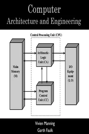 No longer available |Learn more
- (Author)
- 2014(Publication Date)
- College Publishing House(Publisher)
________________________ WORLD TECHNOLOGIES ________________________ Chapter 3 Central Processing Unit Die of an Intel 80486DX2 microprocessor (actual size: 12×6.75 mm) in its packaging. The central processing unit ( CPU ) is the portion of a computer system that carries out the instructions of a computer program, and is the primary element carrying out the computer's functions. The central processing unit carries out each instruction of the program in sequence, to perform the basic arithmetical, logical, and input/output operations of the system. This term has been in use in the computer industry at least since the early 1960s. The form, design and implementation of CPUs have changed dramatically since the earliest examples, but their fundamental operation remains much the same. ________________________ WORLD TECHNOLOGIES ________________________ Early CPUs were custom-designed as a part of a larger, sometimes one-of-a-kind, computer. However, this costly method of designing custom CPUs for a particular application has largely given way to the development of mass-produced processors that are made for one or many purposes. This standardization trend generally began in the era of discrete transistor mainframes and minicomputers and has rapidly accelerated with the popularization of the integrated circuit (IC). The IC has allowed increasingly complex CPUs to be designed and manufactured to tolerances on the order of nanometers. Both the miniaturization and standardization of CPUs have increased the presence of these digital devices in modern life far beyond the limited application of dedicated computing machines. Modern microprocessors appear in everything from automobiles to cell phones and children's toys. History EDVAC, one of the first electronic stored program computers No longer available |Learn more
- (Author)
- 2014(Publication Date)
- Learning Press(Publisher)
________________________ WORLD TECHNOLOGIES ________________________ Chapter 3 Central Processing Unit Die of an Intel 80486DX2 microprocessor (actual size: 12×6.75 mm) in its packaging. The central processing unit ( CPU ) is the portion of a computer system that carries out the instructions of a computer program, and is the primary element carrying out the computer's functions. The central processing unit carries out each instruction of the program in sequence, to perform the basic arithmetical, logical, and input/output operations of the system. This term has been in use in the computer industry at least since ________________________ WORLD TECHNOLOGIES ________________________ the early 1960s. The form, design and implementation of CPUs have changed drama-tically since the earliest examples, but their fundamental operation remains much the same. Early CPUs were custom-designed as a part of a larger, sometimes one-of-a-kind, com-puter. However, this costly method of designing custom CPUs for a particular application has largely given way to the development of mass-produced processors that are made for one or many purposes. This standardization trend generally began in the era of discrete transistor mainframes and minicomputers and has rapidly accelerated with the popularization of the integrated circuit (IC). The IC has allowed increasingly complex CPUs to be designed and manufactured to tolerances on the order of nanometers. Both the miniaturization and standardization of CPUs have increased the presence of these digital devices in modern life far beyond the limited application of dedicated computing machines. Modern microprocessors appear in everything from automobiles to cell phones and children's toys. ________________________ WORLD TECHNOLOGIES ________________________ History EDVAC, one of the first electronic stored program computers.
Index pages curate the most relevant extracts from our library of academic textbooks. They’ve been created using an in-house natural language model (NLM), each adding context and meaning to key research topics.