
eBook - ePub
Sputtering Materials for VLSI and Thin Film Devices
Jaydeep Sarkar
This is a test
Condividi libro
- 608 pagine
- English
- ePUB (disponibile sull'app)
- Disponibile su iOS e Android
eBook - ePub
Sputtering Materials for VLSI and Thin Film Devices
Jaydeep Sarkar
Dettagli del libro
Anteprima del libro
Indice dei contenuti
Citazioni
Informazioni sul libro
An important resource for students, engineers and researchers working in the area of thin film deposition using physical vapor deposition (e.g. sputtering ) for semiconductor, liquid crystal displays, high density recording media and photovoltaic device (e.g. thin film solar cell) manufacturing. This book also reviews microelectronics industry topics such as history of inventions and technology trends, recent developments in sputtering technologies, manufacturing steps that require sputtering of thin films, the properties of thin films and the role of sputtering target performance on overall productivity of various processes. Two unique chapters of this book deal with productivity and troubleshooting issues.
The content of the book has been divided into two sections: (a) the first section (Chapter 1 to Chapter 3) has been prepared for the readers from a range of disciplines (e.g. electrical, chemical, chemistry, physics) trying to get an insight into use of sputtered films in various devices (e.g. semiconductor, display, photovoltaic, data storage), basic of sputtering and performance of sputtering target in relation to productivity, and (b) the second section (Chapter 4 to Chapter 8) has been prepared for readers who already have background knowledge of sputter deposition of thin films, materials science principles and interested in the details of sputtering target manufacturing methods, sputtering behavior and thin film properties specific to semiconductor, liquid crystal display, photovoltaic and magnetic data storage applications.
In Chapters 5 to 8, a general structure has been used, i.e. a description of the applications of sputtered thin films, sputtering target manufacturing methods (including flow charts), sputtering behavior of targets (e.g. current - voltage relationship, deposition rate) and thin film properties (e.g. microstructure, stresses, electrical properties, in-film particles). While discussing these topics, attempts have been made to include examples from the actual commercial processes to highlight the increased complexity of the commercial processes with the growth of advanced technologies. In addition to personnel working in industry setting, university researchers with advanced knowledge of sputtering would also find discussion of such topics (e.g. attributes of target design, chamber design, target microstructure, sputter surface characteristics, various troubleshooting issues) useful.
.
- Unique coverage of sputtering target manufacturing methods in the light of semiconductor, displays, data storage and photovoltaic industry requirements
- Practical information on technology trends, role of sputtering and major OEMs
- Discussion on properties of a wide variety of thin films which include silicides, conductors, diffusion barriers, transparent conducting oxides, magnetic films etc.
- Practical case-studies on target performance and troubleshooting
- Essential technological information for students, engineers and scientists working in the semiconductor, display, data storage and photovoltaic industry
Domande frequenti
Come faccio ad annullare l'abbonamento?
È semplicissimo: basta accedere alla sezione Account nelle Impostazioni e cliccare su "Annulla abbonamento". Dopo la cancellazione, l'abbonamento rimarrà attivo per il periodo rimanente già pagato. Per maggiori informazioni, clicca qui
È possibile scaricare libri? Se sì, come?
Al momento è possibile scaricare tramite l'app tutti i nostri libri ePub mobile-friendly. Anche la maggior parte dei nostri PDF è scaricabile e stiamo lavorando per rendere disponibile quanto prima il download di tutti gli altri file. Per maggiori informazioni, clicca qui
Che differenza c'è tra i piani?
Entrambi i piani ti danno accesso illimitato alla libreria e a tutte le funzionalità di Perlego. Le uniche differenze sono il prezzo e il periodo di abbonamento: con il piano annuale risparmierai circa il 30% rispetto a 12 rate con quello mensile.
Cos'è Perlego?
Perlego è un servizio di abbonamento a testi accademici, che ti permette di accedere a un'intera libreria online a un prezzo inferiore rispetto a quello che pagheresti per acquistare un singolo libro al mese. Con oltre 1 milione di testi suddivisi in più di 1.000 categorie, troverai sicuramente ciò che fa per te! Per maggiori informazioni, clicca qui.
Perlego supporta la sintesi vocale?
Cerca l'icona Sintesi vocale nel prossimo libro che leggerai per verificare se è possibile riprodurre l'audio. Questo strumento permette di leggere il testo a voce alta, evidenziandolo man mano che la lettura procede. Puoi aumentare o diminuire la velocità della sintesi vocale, oppure sospendere la riproduzione. Per maggiori informazioni, clicca qui.
Sputtering Materials for VLSI and Thin Film Devices è disponibile online in formato PDF/ePub?
Sì, puoi accedere a Sputtering Materials for VLSI and Thin Film Devices di Jaydeep Sarkar in formato PDF e/o ePub, così come ad altri libri molto apprezzati nelle sezioni relative a Technology & Engineering e Industrial Engineering. Scopri oltre 1 milione di libri disponibili nel nostro catalogo.
Informazioni
Argomento
Technology & EngineeringCategoria
Industrial EngineeringChapter 1
Sputtering Targets and Sputtered Films for the Microelectronic Industry
A wide variety of materials are sputtered either in pure or in reactive mode to form thin films on chosen substrates for microelectronic applications. Such sputtered thin films are used as silicide contacts, conductors, diffusion barriers, anti-reflection coatings, transparent conducting oxides, reflective layer, semi-reflective layer, dielectric layer, recording media, absorber layer and so forth. In this chapter, commercially important sputtering targets and sputtering chambers (tools) for semiconductor, display, data storage and photovoltaic industries have been identified. This chapter also reviews essential semiconductor, active matrix liquid crystal display (AMLCD), data storage (e.g. magnetic, optical, phase change) and photovoltaic industry topics which include (a) major inventions, (b) technology trends, (c) process flows for device manufacturing, (d) original equipment manufacturers (OEMs) and (e) sputtering target suppliers.
Keywords
Metallization; Interconnect; Thin films; Physical vapor deposition (PVD); PVD tools; Sputtering targets; Semiconductor; Integrated circuits (ICs); Silicide; Salicide; Conductors; Diffusion barriers; Liquid crystal displays; Thin film transistor (TFT); Transparent conducting oxides (TCOs); Indium tin oxide (ITO); Magnetic recording; Inductive head; MR head; GMR head; Longitudinal media; Perpendicular media; Optical storage media; Phase change materials; Photovoltaic devices
1.1 Materials for microelectronics
1.1.1 Introduction
The microelectronic industry arguably uses a wide variety of materials in the form of solid, liquid, gas and gas plasma in microelectronic device components and for the processing of devices. Figure 1.1 shows these elements in the periodic table. Choices for material selection are made based on the applications [1]. With the exception of actinides (the bottom-most row) and a few other unstable and less common elements, most of the elements are used in microelectronics industry. A large number of such elements and their alloys are used in microelectronics devices in the form of thin films [2–20]. Sputtering is one of the techniques for depositing such thin films in which atoms are ejected from a source material by using energetic particles inside a chamber [4,6,14]. In principle, the majority of solid materials can be sputtered under suitable conditions to form thin films. Chapter 2 reviews various sputtering methods for depositing thin films and device technology driven evolution of sputtering equipment (also known as sputtering tools). Sputtering can also be used to remove a thin layer of material from a substrate and this application of sputtering is out of the scope of this book.
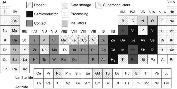
Figure 1.1 Periodic table showing elements and their applications in microelectronic industry [1].
The primary focus of this book is to discuss metallurgy and material science of sputtering materials that are technologically important. These include both: (a) bulk source materials, known as sputtering targets, and (b) deposited thin films for microelectronic applications. Sputtering target can be a conductor, semiconductor or an insulator. Conductivity is one of the key parameters that contrast these three types of solids. As one would expect, a small section of a chapter of this nature has limited scope to cover this subject. Hence, the following sections will only summarize the general characteristics of conduction in conductors, semiconductors and insulators. Afterwards, discussion has been shaped in such a way that readers eventually arrive at those technologically important materials that are sputtered to form thin films for making commercial device such as integrated circuits (ICs), displays, magnetic and optical data storage systems, photovoltaic solar cell and so forth [2–20]. As discussion progresses, readers will note that sputtering is primarily used to deposit metal-based conductors and not so much for semiconductor and insulators (with some exceptions). It is important for readers to note that, in many cases, by the time thin films are sputter deposited on a substrate, a significant amount of investment has already been done for substrate preparation. As a result, any failure at the sputter deposition stage will reduce the overall yield and productivity of the process. For example, in a complementary metal oxide semiconductor (CMOS) chip manufacturing process, by the time a cobalt or nickel film is sputter deposited prior to the silicide formation, active regions have already been formed on the silicon wafer with significant investment.
1.1.1.1 Electrical conductivity
The most common approach to distinguishing conductors, semiconductors and insulators for microelectronic applications is based on their electrical conductivity (reciprocal of resistivity) values. Electrical conductivity (σ) of a material is given by the equation

where n is the number of carriers, q is the charge and μ is the mobility of the carriers. While conductors have high electrical conductivity (104–106 ohm−1 cm−1) insulators have low electrical conductivity (≤10−15 ohm−1 cm−1) and semiconductors have intermediate electrical conductivity (10−6–103 ohm−1 cm−1). These boundaries are not rigid and a certain degree of overlap is possible between these sets of values. In general, the electrical conductivity of the conductors shows a slight but gradual drop with increasing temperature. This is because n is large for conductors and essentially remains unchanged with temperature. Similarly, q remains constant but the mobility term μ decreases slightly with increasing temperature. The mobility of the carriers decreases because of the collision between moving electrons and the phonons (lattice vibrations). Silver, copper and gold are among the best electrical conductors. Transition metals such as iron and nickel are not as good conductors as above metals. However, for semiconductors and the insulators, n increases dramatically with temperature unlike conductors which outweighs the slight decrease in the mobility term. As a result, electrical conductivity of semiconductors increases rapidly with temperature.
Table 1.1 lists the electrical conductivity of some of the common materials at room temperature. Figure 1.2 shows the variation of electrical conductivity in aluminum and germanium with temperature. In fact, insulators are extreme state semiconductors when n is small at normal temperature. In the following sections, a cursory review of the principles of conduction in solids (conductors, semiconductors and insulators) has been presented prior to the discussion of various devices that integrate such materials. Finally, the discussion leads to those conductors, semiconductors and insulators that are sputtered to form films for device fabrication.
Table 1.1
Electrical Conductivity of Selected Bulk Materials
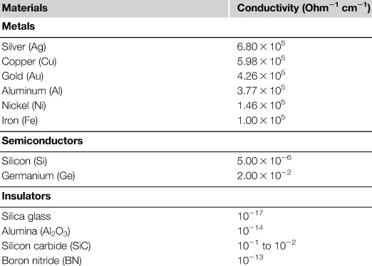
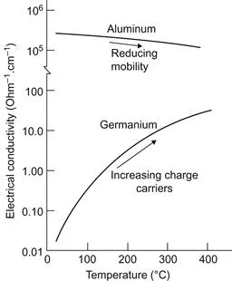
Figure 1.2 Variation of electrical conductivity in aluminum (Al) and germanium (Ge) with temperature.
The electronic behavior of s...