- 783 pages
- English
- ePUB (mobile friendly)
- Available on iOS & Android
eBook - ePub
Optical Diagnostics for Thin Film Processing
About this book
This volume describes the increasing role of in situ optical diagnostics in thin film processing for applications ranging from fundamental science studies to process development to control during manufacturing. The key advantage of optical diagnostics in these applications is that they are usually noninvasive and nonintrusive. Optical probes of the surface, film, wafer, and gas above the wafer are described for many processes, including plasma etching, MBE, MOCVD, and rapid thermal processing. For each optical technique, the underlying principles are presented, modes of experimental implementation are described, and applications of the diagnostic in thin film processing are analyzed, with examples drawn from microelectronics and optoelectronics. Special attention is paid to real-time probing of the surface, to the noninvasive measurement of temperature, and to the use of optical probes for process control.
Optical Diagnostics for Thin Film Processing is unique. No other volume explores the real-time application of optical techniques in all modes of thin film processing. The text can be used by students and those new to the topic as an introduction and review of the subject. It also serves as a comprehensive resource for engineers, technicians, researchers, and scientists already working in the field.
- The only volume that comprehensively explores in situ, real-time, optical probes for all types of thin film processing
- Useful as an introduction to the subject or as a resource handbook
- Covers a wide range of thin film processes including plasma etching, MBE, MOCVD, and rapid thermal processing
- Examples emphasize applications in microelectronics and optoelectronics
- Introductory chapter serves as a guide to all optical diagnostics and their applications
- Each chapter presents the underlying principles, experimental implementation, and applications for a specific optical diagnostic
Trusted by 375,005 students
Access to over 1 million titles for a fair monthly price.
Study more efficiently using our study tools.
Information
CHAPTER 1
Overview of Optical Diagnostics
The thin film industry, which has grown rapidly in recent decades, now affects many diverse areas of manufacturing. Thin film processing is essential to the success of the massive semiconductor and microelectronics industry and to the growth of the emerging optoelectronics industry. These techniques are widely employed for fabricating coatings to produce optical elements, to improve machine tools, and to form protective and anticorrosion layers on many components. Along with this growth has come the development of improved and increasingly sophisticated processes that require a deeper fundamental understanding of the science behind the thin film process. This increased sophistication of processing methods and the ever-increasing complexity of new materials and devices have placed new demands on process engineers, thin film equipment vendors, and product manufacturers. These demands have placed a premium on developing and employing diagnostics to understand these methods in the laboratory and to monitor and control them in the fabrication line. In particular, optical diagnostics have been increasingly used in these applications because of their versatility and power. This book addresses these issues by collecting into one volume descriptions of optical techniques for the in situ analysis, monitoring, and controlling of thin film processes.
The subject of thin film processing is huge, due in part to the plethora of techniques that are commonly used. Films can be deposited, etched, patterned, doped, oxidized, and annealed. Physical and chemical phenomena involving gases, liquids, surface layers, solids, plasmas, and photons can be significant. Many interactions affect the satisfactory progress of the film process. Complex chemistry can occur in the gas and on the surface, and fluid flow can greatly affect performance, as can the appearance of contaminants and undesirable complications, such as the formation of particles. Moreover, each of these processes must be developed and optimized for each material used in manufacturing. These techniques can be quite complicated whether they are being developed for processing simple elements, such as silicon and diamond, or more complex materials, such as the binary semiconductor gallium arsenide and high-temperature superconductors. Given the stringent fabrication specifications regarding film thickness, composition, purity, and crystallinity, the development and application of optical diagnostics for process elucidation and control are clearly essential.
This chapter explores how optical diagnostics can be used to improve thin film processing science and technology. It also serves as a master guide to the rest of the book, interrelating optical methods and their applications as diagnostics. Sections 1.1–1.3 briefly discuss the attributes and characteristics of diagnostics. Section 1.4 details why in situ diagnostics can be essential in thin film processing procedures ranging from investigations of fundamental science to process development and real-time control during manufacturing. In essence, it motivates this entire book. Sections 1.5 and 1.6 respectively survey optical and nonoptical probes. Section 1.7 presents commonly used thin film processing methods and analyzes their diagnostic needs. The tables in this chapter (Tables 1.1–1.10) interrelate diagnostics techniques and their applications, citing as well the sections in which each diagnostic is described.
Table 1.1
Useful in Situ Sensors for Process Control in Representative Integrated Circuit Fabrication Steps*
| Metal CVD | Wafer temperature (real-time) |
| Sheet resistance (endpoint) | |
| Metal film thickness, surface roughness (post-processing) | |
| Dielectric CVD | Wafer temperature (real-time) |
| Film thickness (endpoint) | |
| Particles (in gas, on wafer; real-time, post-processing) | |
| Refractive index, film stress (post-processing) | |
| Silicon CVD/epitaxy | Wafer temperature (real-time) |
| Film thickness (endpoint) | |
| Particles (in gas, on wafer; real-time, post-processing) | |
| Grain size (post-processing) [polycrystalline] | |
| Sheet resistance, surface reflectance (post-processing) | |
| Plasma etch (anisotropic/isotropic, ashing) | Plasma power, plasma density (real-time) |
| Particles (in gas, on wafer; real-time, post-processing) | |
| Film thickness, plasma emission (endpoint) | |
| Critical dimension (real-time, post-processing) [anisotropic etch] | |
| Anisotropy, side-wall angle, overetch (real-time, post-processing) | |
| Selectivity (post-processing) | |
| Thermal oxidation/nitridation | Wafer temperature (real-time) |
| Film thickness, slips, thickness uniformity (post-processing) | |
| Implant activation and drive-in | Wafer temperature, dopant dose and energy (real-time) |
| Electrical activation (endpoint) | |
| Sheet resistance, slips (post-processing) | |
| Resist processing | Resist thickness, uniformity (post-coating, pre-exposure) |
| Latent image, image overlay (during exposure) | |
| Surface condition, plasma emission (dry-develop endpoint) | |
| Critical dimension (post-processing) | |
| Glass reflow | Wafer temperature (real-time) |
| Surface topography (endpoint) | |
| Film thickness, stress (pre- and post-processing) |
*Adapted from Moslehi et al. (1992), © 1992 IEEE, and Barna et al. (1994).
Table 1.2
Methods for Endpoint Detection
| Method | Measuring | Monitoring |
| Optical | ||
| Optical emission spectroscopyab (Section 6.3.1.2) | Spectrum of light emitted from discharge and its intensity | Emission from reactive species and/or etch products |
| Absorptionb(Chapter 8; Section 8.3 for films) | Transmitted light | Change in concentrations in different molecules. |
| Optical reflection (Sections 9.4, 9.5, 9.11) | Reflection changes, interference effects,bc or ellipsometry parameter monitoring | Changes in film thickness |
| Scatterometryb (Section 11.2) | Diffracted light | The profile of the surface or of the refractive index distribution. |
| Pyrometry (thermal imaging) (Section 13.2) | Infrared emission | Changes in emissivity |
| Photoemission optogalvanic spectroscopya (Section 17.3) | Plasma current | Changes in work function due to changed surface |
| Nonoptical | ||
| Mass spectrometry | Gas composition | Etch products |
| Impedance monitoringa | Impedance mismatch | Voltage change |
| Langmuir probea | Changes in electron density or average energy | Current from probe |
| Pressure | Total pressure | Changes in total pressure |
aUseful only during plasma etching (Marcoux and Foo, 1981).
bUseful for evaluating resist processing.
cInterference effects in OES (Section 6.3.1.3), Raman scattering (Section 12.4.2), and pyrometry (Section 13.4) can also be used for endpoint detection.
Table 1.3
Optical Diagnostics of Surfaces
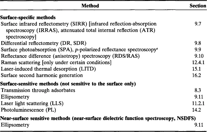
aAlso known as Brewster-angle reflection spectroscopy (BARS).
Table 1.4
Probes for Gas-Phase Species Identification and Density Measurements*
| Method | Section |
| OESa | 6.3 |
| LIF | 7.2 |
| Infrared diode laser absorption spectroscopy (IR-DLAS) | 8.2.1.1 |
| Fourier transform infrared spectroscopy (FTIRS) | 8.2.1.2 |
| Ultraviolet/visible absorption | 8.2.2 |
| Interference holography | 10.1 |
| Raman scattering | 12.3 |
| CARS | 16.1 |
| Third harmonic generation (THG) | 16.3 |
| REMPI | 17.1 |
*See Table 1.5 for pr...
Table of contents
- Cover image
- Title page
- Table of Contents
- Copyright
- Dedication
- Preface
- Notations and Symbols
- Chapter 1: Overview of Optical Diagnostics
- Chapter 2: The Properties of Light
- Chapter 3: The Structure of Matter
- Chapter 4: Interactions of Light with Matter for Spectroscopy
- Chapter 5: Diagnostics Equipment and Methods
- Chapter 6: Optical Emission Spectroscopy
- Chapter 7: Laser-Induced Fluorescence
- Chapter 8: Transmission (Absorption)
- Chapter 9: Reflection
- Chapter 10: Interferometry and Photography
- Chapter 11: Elastic Scattering and Diffraction from Particles and Nonplanar Surfaces (Scatterometry)
- Chapter 12: Raman Scattering
- Chapter 13: Pyrometry
- Chapter 14: Photoluminescence
- Chapter 15: Spectroscopies Employing Laser Heating
- Chapter 16: Nonlinear Optical Diagnostics
- Chapter 17: Optical Electron/Ion Probes
- Chapter 18: Optical Thermometry
- Chapter 19: Data Analysis and Process Control
- Index
Frequently asked questions
Yes, you can cancel anytime from the Subscription tab in your account settings on the Perlego website. Your subscription will stay active until the end of your current billing period. Learn how to cancel your subscription
No, books cannot be downloaded as external files, such as PDFs, for use outside of Perlego. However, you can download books within the Perlego app for offline reading on mobile or tablet. Learn how to download books offline
Perlego offers two plans: Essential and Complete
- Essential is ideal for learners and professionals who enjoy exploring a wide range of subjects. Access the Essential Library with 800,000+ trusted titles and best-sellers across business, personal growth, and the humanities. Includes unlimited reading time and Standard Read Aloud voice.
- Complete: Perfect for advanced learners and researchers needing full, unrestricted access. Unlock 1.4M+ books across hundreds of subjects, including academic and specialized titles. The Complete Plan also includes advanced features like Premium Read Aloud and Research Assistant.
We are an online textbook subscription service, where you can get access to an entire online library for less than the price of a single book per month. With over 1 million books across 990+ topics, we’ve got you covered! Learn about our mission
Look out for the read-aloud symbol on your next book to see if you can listen to it. The read-aloud tool reads text aloud for you, highlighting the text as it is being read. You can pause it, speed it up and slow it down. Learn more about Read Aloud
Yes! You can use the Perlego app on both iOS and Android devices to read anytime, anywhere — even offline. Perfect for commutes or when you’re on the go.
Please note we cannot support devices running on iOS 13 and Android 7 or earlier. Learn more about using the app
Please note we cannot support devices running on iOS 13 and Android 7 or earlier. Learn more about using the app
Yes, you can access Optical Diagnostics for Thin Film Processing by Irving P. Herman in PDF and/or ePUB format, as well as other popular books in Technology & Engineering & Condensed Matter. We have over one million books available in our catalogue for you to explore.