![]()
Chapter 1
Introduction
A nanometer (nm) is one billionth (10-9) of a meter. Nanoscience can be defined as the science of objects and phenomena occurring at the scale of 1 to 100 nm. The range of 1–100 nm was taken as the defining range by the US National Science and Technology Council in its report titled “National Nanotechnological Initiative: Leading to the Next Industrial Revolution”, in February 2000 and a subsequent report in 2004. The committee noted that “Nanotechnology is the understanding and control of matter at dimensions of roughly 1 to 100 nanometers, where unique phenomena enable novel applications. ....At this level, the physical, chemical, and biological properties of materials differ in fundamental and valuable ways from the properties of individual atoms and molecules of bulk matter” [1]. It was also mentioned that “novel and differentiating properties and functions are developed at a critical length scale of matter typically under 100 nm”. Actually, in most cases, this happens below 10 nm. On the other hand, some nanoscale phenomena extend beyond 100 nm. The range of 1 to 100 nm appears therefore to be appropriate for the purpose of defining the field as long as it is kept in mind that in some cases one may have to step across these boundaries.
Although the field of nanoscience and nanotechnology has consolidated and emerged as a distinct field only in the decades of eighties and nineties, the activities encompassed by the field have been carried on for decades and in fact for centuries prior to that. Some prominent examples are the use of noble metal particles to impart beautiful colors to the windows of the medieval cathedrals (dating back to fourth century CE), explanation of this effect by Gustav Mie in 1908, development of the ferrofluids in the 1960s, discovery of the magic numbers in the metal clusters in the 1970s, fabrication of the quantum wells in 1970s and many such developments including the development of photography and catalysis.
In 1959 Richard Feynman delivered his famous talk at Caltech titled “There is plenty of room at the bottom” [2]. In it Feynman visualized building of nanosized circuits for use in computers and using precisely positioned assembly of atoms to store vast amounts of information. The Feynman’s talk was much ahead of its time — the field of nanoscience and nanotechnology can be said to have come into its own only in the 1990s. The development of newer characterization tools such as the scanning probe microscope and the atomic force microscope and the technique of electron beam lithography capable of making 10 nm structures in 1980s contributed much to the development of the field.
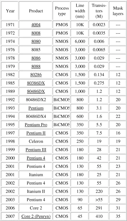
Another factor which provided a great impetus to the area was the need of the computer chip industry. The manufacture of integrated circuits used in the electronics industry is at present carried out by the so called “top down” method in which a thin film is first deposited and parts of it are then etched away to yield the desired pattern. The feature size on the integrated circuits that can be produced by this method has exponentially decreased over the years as predicted by Moore in 1965 [3, 4]. Table 1.1 illustrates this by showing how the line width and the number of transistors per chip in the microprocessors have changed over the years. The number of transistors per chip has increased from 2300 per chip in 1971 to 410 million in 2007 — an increase by a factor of 200,000! This is roughly in accordance with the prediction of Moore that the number of transistors that are placed on a chip should double approximately every two years. Continuing with this trend would mean that the transistor size would have to be scaled down to 9 nm by the year 2016 and to still lower size after that. Photolithography with excimer laser is currently used to fabricate integrated circuits with features below 45 nm and this trend is expected to continue to reach a feature size of about 10 nm. It is apparent that to sustain the growth of the massive semiconductor industry the feature size on the chips will have to be reduced to a few nanometers and new techniques will be needed to accomplish this.
The strategies that are going to be adapted for going below 10 nm are not yet clear. The bottom–up approach in which a structure is assembled from elementary building blocks using noncovalent interactions is of considerable interest. Bottom–up self–assembly is the way all the plant and biological structures are made. These are hierarchical structures which start out from a simple nanostructure and combine to form a higher level building block; these building blocks further assemble to give the next level of structure and so on. The connective tissue in the body is a hierarchical structure consisting of many levels of assembly. The beautiful colors and iridescence seen in the wings of butterflies and the feathers of many birds such as a peacock arise due to specific nanostructures created by nature using the bottom–up self assembly. Nanotechnologists derive inspiration form these natural nanostructures to design useful nanomaterials. Such materials are called biomimetic materials.
Table 1.1. Microprocessor trends (reproduced with permission from IC Knowledge LLC)
The zero dimensional nanostructures and nanomaterials are defined as those in which all the three dimensions are less than 100 nm. Similarly in the one and two dimensional nanostructures, two and one dimensions are < 100 nm, respectively. Typical examples of the zero, one and two dimensional nanostructures are semiconductor quantum dots, carbon nanotubes and quantum well structures respectively.
The bulk nanostructured materials are those materials which are synthesized in bulk quantities (i.e. > mm3) and have structural features which are controllable at the nanoscale. Examples are nanocrystalline metals and composites of clay or carbon nanotubes with polymers or other matrices.
In the nanomaterials, the surface to volume ratio is very high and increases rapidly as the relevant dimension decreases. For a 3 nm diameter particle approximately 90 % of the atoms reside on the surface. The result is that the surfaces play an increasingly important role in determining the properties of nanomaterials. In the next chapter (Chapter 2), we first discuss the structure and properties of surfaces and illustrate this with some examples of their application to nanostructures. As an illustration, the use of nanostructuring of surfaces to render them superhydrophobic or superhydrophilic is discussed.
Apart from the issue of fabrication of nanomaterials, another issue which has to be faced is the new phenomena which arise when the size is scaled down to such levels. For example in the integrated circuits the quantum tunneling becomes important and the conventional circuits may no longer work. The changes in the properties of materials with size in the range of 1 to 100 nm is a key issue in Nanoscience. Such changes in properties begin to occur when the size approaches a characteristic scaling length which is usually different for each property or phenomenon. Many of these changes, e.g. those in the electronic and optical properties, arise due to quantum effects. A review of some topics in physics and a discussion of the various scaling lengths is given in Chapter 3 to help understand such changes in properties.
The first example of the zero dimensional nanomaterials, the semiconductor quantum dots, is discussed in Chapter 4. The nanostructures in which the carriers (electrons and holes) are confined within nanometer sized regions in all three dimensions are called quantum dots. This confinement leads to effects such as a change in the band gap and Coulomb blockade. These effects together with the principles involved in the fabrication of self assembled quantum dots is described in Chapter 4.
One manifestation of the change in the band gap of the semiconductor quantum dots with size is the appearance of distinct size dependent colors in the suspensions of these particles. The suspensions of the nanoparticles of some metals also show bright colors; however, the source of this is a different phenomenon called the surface plasmon resonance. This is discussed in Chapter 5.
Several characteristic length scales in the nanometer range exist in magnetism. An important length scale for the magnetic phenomena at nanoscale is the domain size in ferromagnetic crystals. Typically the domain size is in the range 10–200 nm. One of the important effects that is observed as a result of this is the phenomenon of superparamagnetism in nanometer sized ferromagnetic crystals. The phenomenon of giant magnetic resistance arises due to the spin of the electrons and is observed in a stack of alternating, nanometer thick, magnetic and nonmagnetic layers. The ability to control and manipulate the spins of electrons, has given rise to the whole new field of spin based electronics or spintronics where the electron carries not only the charge but also information in the form of its spin. In Chapter 6, some of these topics are discussed. The chapter ends with a brief discussion of spintronics and the applications of superparamagnetic and other materials.
Colloids can be defined as systems which are microscopically heterogeneous and in which one component has at least one of its dimensions in the range between 1 nm and 1 μm. A model colloidal system is a suspension of particles having diameters ranging from 1 nm to 1 μm in a liquid. Such suspensions are of interest in nanotechnology in the preparation of nanoparticles, their modification and their assembly to yield nanomaterials and nanodevices. In order for the particles to remain suspended (i.e. for the dispersion to be stable) for any useful length of time despite the van der Waal’s attraction, the presence of a repulsive force between them is essential. Such repulsive interaction is produced either by the presence of electrical charges or by the adsorption of some polymers on the particle surface. The stabilization of a dispersion by these techniques is called electrostatic stabilization and steric stabilization respectively. In chapter 7 these interactions are first discussed. Secondly, the example of colloidal crystals is used to illustrate the use of nanoparticles in the fabrication of nanostructures.
The carbon nanostructures — graphenes, fullerenes and carbon nanotubes — have remarkable properties making them useful for a large number of applications. In chapter 8 the structure, preparation, properties and some potential applications of these nanostructures are discussed.
The layer structure of graphite is conducive for the growth of fullerenes and one dimensional carbon nanotubes. By folding into tubes or spheres the dangling bonds at the edges of a graphene sheet are eliminated making the structure more stable. This holds true for other layered structures also. The chalcogenides of metals such as tungsten or molybdenum are well known inorganic layered structures. Indeed the first noncarbon nanotubes to be observed consisted of MoS2 and WS2.
After the discovery of carbon nanotubes, efforts were intensified to prepare nanotubes of other materials. Although, the layered inorganic compounds were the first ones to be explored because of the similarity with graphite, at present synthesis strategies are available to produce one dimensional nanostructures from almost any material. Nanowires of materials other than carbon are dealt in Chapter 9.
The two dimensional (2D) nanostructures are defined as structures in which two dimensions (say along the x and y axes) are large while the third dimension along the z axis is less than 100 nm. Preparation of the 2D nanostructures is carried out by the techniques of thin film deposition. Thin film deposition is a key process in nanotechnology. In addition to the direct formation of the 2D nanostructures, thin film deposition is used for the preparation of core–shell particles, hollow shells, functionalization of particles and surfaces, and other miscellaneous structures. In chapter 10 the various deposition techniques and their applications in 2-D nanostructures are discussed and one important example, multilayers for mechanical engineering applications, is discussed in some detail.
The bulk nanostructured materials such as nanocrystalline metals and ceramics and nanocomposites have the potential to offer materials with extremely high strengths and other mechanical properties. The polycrystalline metals show a deviation from the expected trends in properties as the grain size goes below a few nanometers. Thus the hardness and the strength of a polycrystalline metal increase with decreasing grain size as (grain size)-1/2 according to the well known Hall- Petch relation. However, there is a change in behavior when the grain size approaches a few nanometers. Such changes in the properties of nanocrystalline solids are discussed in this Chapter 11. In Appendix II, an introduction to the mechanical properties of solids is provided.
A composite is a material made from two chemically distinct materials which maintain their identity and have a distinct interface between them in the finished structure. The mechanical properties of a composite are a strong function of the properties of the reinforcement. From this point of view, the carbon nanotubes (CNT) with a Young’s modulus of 600 to 1000 GPa, strength ranging from 35 to 110 GPa and a density as low as 1.3 gcm-3 can be said to be the ultimate reinforcement material. The polymer–CNT composites are of special interest because of their low density for applications such as aerospace and automobile where weight saving is a very important concern.
In addition to the CNT, several other nanofillers have been used to prepare nanocomposites. Most important amongst these are the composites of polymer with exfoliated clay particles. In Chapter 12, after discussing some basic ideas about composites, the polymer–CNT and the polymer–clay nanocomposites are discussed.
Soft materials such as polymers have come to occupy a special place in nanoscience and nanomaterials. In Chapter 13 some important classes of molecules widely used in soft matter are briefly discussed. These are polymers and biopolymers, surfactants and dendrimers. These are also of relevance to the topic of self assembly discussed in the following chapter.
As mentioned earlier, one of the approaches being investigated to assemble nanosized structures is the self assembly process. In this process the aim is to assemble a structure starting from some building blocks. In contrast to the strong covalent or other primary bonds that are used in the synthesis of a molecule, it is the much weaker secondary bonds that are used in the self assembly process. The weak bonds permit self correction of any defects during the assembly process because such bonds can be easily broken and remade to create a structure with the lowest free energy. The self assembly process thus operates under the “thermodynamic control”. In Chapter 14, the various secondary interactions that are made use of in the self assembly are first described. This is followed by a discussion of some important examples.
![]()
Chapter 2
Surfaces
2.1 Introduction
The surface of an object becomes increasingly important as its size decreases. Generally the surface effects extend to a depth of few atoms below the surface. A plot of the fraction of atoms on the surface of a cubic crystal with a lattice parameter of 0.2 nm and assuming that the surface layer extends to a depth of 4 atoms from the surface is shown in Fig. 2.1. It is seen that the number of atoms on the surface increases rapidly for particle size d < 10 nm and reaches ~ 90% for d = 3 nm. This shows that a majority of atoms in a nanoparticle reside on its surface. The surface atoms differ from the bulk atoms in many ways. The coordination number of a surface atom is smaller than that of a bulk atom i.e. a surface atom has unsatisfied bonds which make it chemically very active. Therefore, the chemical activity of a material increases drastically as the particle size reaches a few nm. A dramatic manifestation of this is the auto ignition of fine metal powders in air. Because of a smaller coordination number, ...