
eBook - ePub
Nanotechnology for Microelectronics and Optoelectronics
Raúl José Martín-Palma,José Martínez-Duart,Fernando Agullo-Rueda
This is a test
Partager le livre
- 304 pages
- English
- ePUB (adapté aux mobiles)
- Disponible sur iOS et Android
eBook - ePub
Nanotechnology for Microelectronics and Optoelectronics
Raúl José Martín-Palma,José Martínez-Duart,Fernando Agullo-Rueda
Détails du livre
Aperçu du livre
Table des matières
Citations
À propos de ce livre
When solids are reduced to the nanometer scale, they exibit new and exciting behaviours which constitute the basis for a new generation of electronic devices.
Nanotechnology for Microelectronics and Optoelectronics outlines in detail the fundamental solid-state physics concepts that explain the new properties of matter caused by this reduction of solids to the nanometer scale. Applications of these electronic properties is also explored, helping students and researchers to appreciate the current status and future potential of nanotechnology as applied to the electronics industry.
- Explains the behavioural changes which occur in solids at the nanoscale, making them the basis of a new generation of electronic devices
- Laid out in text-reference style: a cohesive and specialised introduction to the fundamentals of nanoelectronics and nanophotonics for students and researchers alike
Foire aux questions
Comment puis-je résilier mon abonnement ?
Il vous suffit de vous rendre dans la section compte dans paramètres et de cliquer sur « Résilier l’abonnement ». C’est aussi simple que cela ! Une fois que vous aurez résilié votre abonnement, il restera actif pour le reste de la période pour laquelle vous avez payé. Découvrez-en plus ici.
Puis-je / comment puis-je télécharger des livres ?
Pour le moment, tous nos livres en format ePub adaptés aux mobiles peuvent être téléchargés via l’application. La plupart de nos PDF sont également disponibles en téléchargement et les autres seront téléchargeables très prochainement. Découvrez-en plus ici.
Quelle est la différence entre les formules tarifaires ?
Les deux abonnements vous donnent un accès complet à la bibliothèque et à toutes les fonctionnalités de Perlego. Les seules différences sont les tarifs ainsi que la période d’abonnement : avec l’abonnement annuel, vous économiserez environ 30 % par rapport à 12 mois d’abonnement mensuel.
Qu’est-ce que Perlego ?
Nous sommes un service d’abonnement à des ouvrages universitaires en ligne, où vous pouvez accéder à toute une bibliothèque pour un prix inférieur à celui d’un seul livre par mois. Avec plus d’un million de livres sur plus de 1 000 sujets, nous avons ce qu’il vous faut ! Découvrez-en plus ici.
Prenez-vous en charge la synthèse vocale ?
Recherchez le symbole Écouter sur votre prochain livre pour voir si vous pouvez l’écouter. L’outil Écouter lit le texte à haute voix pour vous, en surlignant le passage qui est en cours de lecture. Vous pouvez le mettre sur pause, l’accélérer ou le ralentir. Découvrez-en plus ici.
Est-ce que Nanotechnology for Microelectronics and Optoelectronics est un PDF/ePUB en ligne ?
Oui, vous pouvez accéder à Nanotechnology for Microelectronics and Optoelectronics par Raúl José Martín-Palma,José Martínez-Duart,Fernando Agullo-Rueda en format PDF et/ou ePUB ainsi qu’à d’autres livres populaires dans Technologie et ingénierie et Ingénierie de l'électricité et des télécommunications. Nous disposons de plus d’un million d’ouvrages à découvrir dans notre catalogue.
Informations
Chapter 1
Mesoscopic Physics and Nanotechnologies
1.1 Outlook of the book
1.2 Trends in nanoelectronics and optoelectronics
1.3 Characteristic lengths in mesoscopic systems
1.4 Quantum mechanical coherence
1.5 Quantum wells, wires, and dots
1.6 Density of states and dimensionality
1.7 Semiconductor heterostructures
1.8 Quantum transport
References
Further Reading
Problems
1.1 OUTLOOK OF THE BOOK
The interest in the study of the physical properties of electronic materials of very small sizes, usually in the nanometre range, resides in various factors. One of them is due to the trends in microelectronic integrated devices, for which smaller sizes imply operation at higher frequencies, higher functionality, lower fabrication costs for a given performance, etc. A second reason, more important from a scientific point of view, is related to the appearance of new fundamental physical effects, such as resonant tunnelling, quantum conductance, Coulomb blockade, Hall quantum effects, etc. In addition, very frequently, these fundamental discoveries are related to practical devices like quantum well lasers, single electron transistors, confined quantum Stark effect optical modulators, etc.
In Chapter 1 of this book, we start by reviewing the present trends of microelectronic and optoelectronic semiconductor devices, which are the basis for the new field of nanoelectronics. After this we will revise a series of concepts of mesoscopic physics, such as characteristic lengths, needed for the definition of nanostructures. We will also set up the physical basis of semiconductors of reduced dimensionality: quantum wells (2D), quantum wires (1D), and quantum dots (0D). We are aware that some of the concepts introduced in this chapter will be difficult for some readers to grasp, especially if confronted to them for the first time. However, we think that overall it is advantageous to get acquainted with them from the very beginning. After this introductory chapter, a survey of the concepts of quantum mechanics, solid state, and semiconductor physics is presented in Chapters 2 and 3. Chapter 4 deals with the physics of low-dimensional semiconductors, i.e. quantum wells, wires, and dots. In Chapter 5, some of the most frequently used quantum heterostructures are revised, as well as superlattices. The effects of electric and magnetic fields on nanostructures are studied in Chapters 6 and 7, giving special emphasis to the quantum conductance and the quantum Hall effect. The rich variety of optical processes in semiconductor nanostructures is treated in Chapter 8, which completes the basic physical properties of the mesoscopic systems. The last two chapters of the book deal with the electronic and optoelectronic semiconductor devices. In Chapter 9, several kinds of high-frequency diodes and transistors, based on resonant tunnelling and single electron effects, are illustrated. Finally, Chapter 10 is dedicated to the optoelectronic and photonic devices which use quantum heterostructures: quantum well lasers, photodetectors, and optical modulators.
1.2 TRENDS IN NANOELECTRONICS AND OPTOELECTRONICS
The evolution of microelectronic devices is influenced by factors such as growing demands in memory capacity of integrated circuits, high transmission data speed, optical communications, etc. This requires electronic devices with faster speed operation and smaller size, as is the case of silicon integrated circuits, in particular dynamic random access memories (DRAMs). Figure 1.1 shows the reduction of feature size of metal-oxide-semiconductor (MOS) transistors, as well as the number of bits per chip for the period 1970–2000 [1]. For example, a 256 M-bit DRAM contains about 109 transistors with a feature size L close to 100 nm. For structures with these dimensions, transport can still be treated classically, but we are already at the transition regime to quantum transport (Section 1.8). Today it is believed that present silicon technology will evolve towards feature sizes still one order of magnitude lower, i.e. L ∼ 10 nm; but below this size, transistors based on new concepts like single electron transistors, resonant tunnelling devices, etc. (Chapter 9) will have to be developed. The operation of this new kind of devices has to be described by the concepts of mesoscopic and quantum physics. It is interesting to remark that quantum effects show up in III-V devices for larger feature sizes, as a consequence of the smaller value of the effective mass, and therefore larger value of the de Broglie wavelength (Section 1.3).
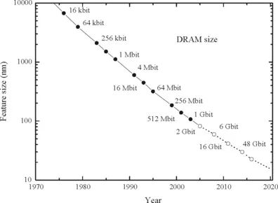
Figure 1.1 Evolution of the minimum feature size of a Si DRAM. After [1].
In the near future, and due to the growing demands of calculus from industries like communications, information, military, space, etc. microelectronics will be replaced by nanoelectronics since the feature size of electronic devices will be reduced to about 10 nm. Although there has been an impressive advance at the device and technology level during the last decade, the progress in the development of new system architectures dealing with billions of transistors is scarce. In this sense, new architectures for parallel data processing are under current development.
The evolution towards nanoelectronics has been possible because of advances in the deposition of very thin films to form heterostructures in which electrons could be confined to a 2D mesoscopic system. Standard evaporation and sputtering techniques did not produce heter...