Technology & Engineering
Logic Gates
Logic gates are fundamental building blocks of digital circuits, performing logical operations on one or more binary inputs to produce a single binary output. The basic types of logic gates include AND, OR, NOT, NAND, NOR, and XOR gates, each with its own unique function and truth table. These gates are essential for designing and constructing complex digital systems and computers.
Written by Perlego with AI-assistance
Related key terms
1 of 5
12 Key excerpts on "Logic Gates"
 eBook - PDF
Introduction To Computers NQF2 SB
TVET FIRST
- Sparrow Consulting(Author)
- 2013(Publication Date)
- Macmillan(Publisher)
A logic gate is a physical electronic component that forms part of the computer’s circuitry which can manipulate an input signal to give a desired output signal. Most Logic Gates take in two or more inputs of binary values and produce one output with a value of 1 or 0. We usually use the letters A, B, C, and so on, to label inputs, and F, Q or Z to label the output. However, you can use any letters. It is common practice to explain the function of a logic circuit with a related circuit that uses switches with a power source and a light. When the light is on the value is considered to be ‘high’, ‘on’ or ‘1’. When the light is off it indicates a ‘low’, ‘off’ or a ‘0’. Refer to Fig. 1.2 and study the circuits. The first one shows an AND gate. If you look at the AND gate switch representation, you will see that all the switches must be turned ‘on’, (‘high‘ or ‘1’) before the light will light up or become ‘high’. Because it uses four switches as input, the AND gate that is represented here is indicated inside the circuit as an AND gate with four inputs. The second symbol inside the circuit is the IEC (International Electrotechnical commission) symbol for an AND gate. The second circuit explains how the OR gate works. In this case any one of the switches that is turned ‘on’, (goes ‘high’ or ‘1’) will cause the light as the output to go ‘high’. Once again the symbols for the OR gate are shown inside the switch circuit. The last gate is a NAND gate. An easy way of remembering the NAND gate is to read it as a Not AND gate. The Not relates to the little circle on the output side of the gate. The AND part of the gate functions like any AND gate in which all the inputs need to be ‘on’ for an output of ‘1’. The little circle represents an inverter, which turns a ‘1’ into a ‘0’ and a ‘0’ into a ‘1’. The result is that when all the inputs are ‘0’ the output of the NAND gate will be ‘1’. eBook - PDF
Mechatronics
An Integrated Approach
- Clarence W. de Silva(Author)
- 2004(Publication Date)
- CRC Press(Publisher)
10.3.1 Logic Gates Logic Gates are the basic circuit elements found in IC circuits that are used in digital systems. A logic gate has one or more logical inputs and only one logical output. Each input line or output line of the gate can have one of two states: true (represented by the binary digit 1) and false (represented by the binary digit 0). It is easy to see how a combination of switches can be used to form a logic gate. For example, two switches connected in series can serve as an AND gate because current passes through the circuit only when both switches are closed. Output of the gate is the state of the circuit. Hence, by denoting the closed-circuit state as true (1) and the open-circuit state as false (0), we can obtain a truth table for the AND gate, as shown in Figure 10.3(a). Note that the gate has two inputs, which are the states of the two switches. Similarly, an OR gate can be formed by connecting two switches in parallel, as shown in Figure 10.3(b). In this OR gate, the output state is considered true (1) also when both inputs are true simultaneously. Alternatively, in an EXCLUSIVE OR (XOR), the output state is taken as false (0) when both inputs are true, and the output is true when only one of the inputs is true. Mechanical switches and relays are not suitable for Logic Gates in digital circuits. Solid-state switches are the preferred variety. Semiconductor elements such as diodes and transistors can function as solid-state switches. In digital systems, these elements are present in the IC form and not in their discrete component form. The three basic Logic Gates are AND, OR, and NOT. The three gates NAND, XOR, and NOR can be constructed from the first three gates, but all six of these gates may be FIGURE 10.3 Examples of basic Logic Gates formed using switches: (a) AND gate and its truth table; (b) OR gate and its truth table. eBook - ePub
- Julio Sanchez, Maria P. Canton(Authors)
- 2017(Publication Date)
- CRC Press(Publisher)
Chapter 3 Logic Gates and Circuit Components 3.1 Logic GatesA logic gate can be a virtual or a physical device. In either case the logic gate takes one or more binary signals as input and produces a binary output as a logical function. The basic logical operations of AND, OR, XOR, and NOT are described in basic electronics and Boolean algebra texts. Although Logic Gates can be made from electromagnetic relays, mechanical switches, or optical components, nowadays they are normally implemented using diodes and transistors.Charles Babbage’s Analytical Engine, devised around 1837, used mechanical Logic Gates based on gears. Electromagnetic relays were later used for Logic Gates, and these were eventually replaced by vacuum tubes, as Lee De Forest’s modification of the Fleming valve can be used as an AND logic gate. In 1937, Claude E. Shannon wrote a thesis paper that introduced the use of Boolean algebra in the analysis and design of switching circuits. The first modern electronic gate was invented by Walther Bothe in 1924, for which he received part of the 1954 Nobel prize in physics.The primitive types of gate are the AND, OR, and NOT. Additionally, the XOR gate offers an alternative version of the OR. All other Boolean operations can be implemented by combining the three primitive types. However, for convenience, other secondary types have been developed. These are called NAND (NOT plus AND), NOR (NOT plus OR), and XNOR (XOR plus NOT). The advantage of these secondary Logic Gates is that they require fewer circuit elements for a given function. In fact, the NAND gate is the simplest of all gates, except for the NOT gate. Furthermore, a NAND can implement both a NOT and an OR function; therefore it can replace AND, OR, and NOT. This means that the NAND gate is the only type actually needed in a real system. Programmable logic arrays will very often contain nothing but NAND gates. The symbols for Logic Gates are shown in Figure 3-1 eBook - PDF
Digital Electronics
Principles, Devices and Applications
- Anil K. Maini(Author)
- 2007(Publication Date)
- Wiley(Publisher)
Each one of the basic Logic Gates is a piece of hardware or an electronic circuit that can be used to implement some basic logic expression. While laws of Boolean algebra could be used to do manipulation with binary variables and simplify logic expressions, these are actually implemented in a digital system with the help of electronic circuits called Logic Gates. The three basic Logic Gates are the OR gate, the AND gate and the NOT gate. 4.3.1 OR Gate An OR gate performs an ORing operation on two or more than two logic variables. The OR operation on two independent logic variables A and B is written as Y = A + B and reads as Y equals A OR B and not as A plus B . An OR gate is a logic circuit with two or more inputs and one output. The output of an OR gate is LOW only when all of its inputs are LOW. For all other possible input combinations, the output is HIGH. This statement when interpreted for a positive logic system means the following. The output of an OR gate is a logic ‘0’ only when all of its inputs are at logic ‘0’. For all other possible input combinations, the output is a logic ‘1’. Figure 4.3 shows the circuit symbol and the truth table of a two-input OR gate. The operation of a two-input OR gate is explained by the logic expression Y = A + B (4.1) As an illustration, if we have four logic variables and we want to know the logical output of ( A + B + C + D , then it would be the output of a four-input OR gate with A , B , C and D as its inputs. Y=A+B A B A 0 0 1 1 B 0 1 0 1 Y 0 1 1 1 Figure 4.3 Two-input OR gate. 72 Digital Electronics Y=A+B+C A B C (a) Y=A+B+C+D A C (b) D A 0 0 0 0 1 1 1 1 B 0 0 1 1 0 0 1 1 C 0 1 0 1 0 1 0 1 Y 0 1 1 1 1 1 1 1 (c) B Figure 4.4 (a) Three-input OR gate, (b) four-input OR gate and (c) the truth table of a three-input OR gate. Figures 4.4(a) and (b) show the circuit symbol of three-input and four-input OR gates. Figure 4.4(c) shows the truth table of a three-input OR gate. eBook - PDF
- S Sasti D Sasti(Author)
- 2019(Publication Date)
- Macmillan(Publisher)
There are 8 columns, C1–C8. l After reading the decision table, we can see that, based on 8 sequences of inputs represented by the columns, we will get only four 1s or Yes or On results. l The final result is represented in row 8. Unit 1.5: Logic Gates 1.5.1 Logic Gates A computer is an electronic device made up of electronic circuits that perform different actions. A logic gate is the building block of these circuits. Logic Gates are devices that are based on the logical operators we studied in previous units. We can now take a Boolean expression and express it diagrammatically in the form of a logic circuit. We use symbols to represent the different gates. Table 1.9 shows the symbols and truth tables for the various Logic Gates. Table 1.9: Logic gate symbols and truth tables Logic gate Symbol Truth table NOT gate A Q A Q 0 1 1 0 AND gate A Q B Inputs Outputs A B Q = A AND B 0 0 0 0 1 0 1 0 0 1 1 1 11 Module 1 Logic gate Symbol Truth table OR gate A Q B Inputs Outputs A B Q = A OR B 0 0 0 0 1 1 1 0 1 1 1 1 NAND gate A Q B Inputs Outputs A B Q = A NAND B 0 0 1 0 1 1 1 0 1 1 1 0 NOR gate A Q B Inputs Outputs A B Q = A NOR B 0 0 1 0 1 0 1 0 0 1 1 0 Exclusive OR (XOR) gate A Q B Inputs Outputs A B Q = A XOR B 0 0 0 0 1 1 1 0 1 1 1 0 The new logical operators in Table 1.9 are the NAND, NOR and XOR operators: l NAND: Represents NOT AND. It evaluates the inputs with the AND operator and then reverses the result. l NOR: Represents NOT OR. It evaluates the inputs with the OR operator and then reverses the result. l XOR: We will discuss the XOR operator in the next section. Each gate may have two or more inputs, except for the NOT gate (inverter) which works on a single input. The logic gate symbols for the negating operators (NOT, NOR, NAND) have a small circle at the end of the gate. 12 Topic 1 Example 1.6: Designing logic circuits from Boolean expressions Draw the circuit for the following Boolean expressions: 1. eBook - PDF
Digital Logic
With an Introduction to Verilog and FPGA-Based Design
- M. Rafiquzzaman, Steven A. McNinch(Authors)
- 2019(Publication Date)
- Wiley(Publisher)
53 Digital Logic with an Introduction to Verilog and FPGA-Based Design. First Edition. M. Rafiquzzaman and Steven A. McNinch. © 2019 John Wiley & Sons, Inc. Published 2019 by John Wiley & Sons, Inc. 3 DIGITAL Logic Gates, BOOLEAN ALGEBRA, AND SIMPLIFICATION Digital circuits contain hardware elements called “gates” that perform logic operations on binary numbers. Devices such as transistors can be used to perform the logic operations. Boolean algebra is a mathematical system that provides the basis for these logic operations. George Boole, an English mathematician, introduced this theory of digital logic. The term Boolean Variable is used to mean the two-valued binary digit 0 or 1. This chapter describes fundamentals of digital Logic Gates, basic logic operations, Boolean algebra, and minimization of Boolean functions using identities. Finally, topics such as Concensus theorem, glitches in combinational circuits, obtaining complement of a Boolean function, and XOR/ XNOR operations are also included. 3.1 Basic Logic Operations Boolean algebra uses three basic logic operations namely, NOT, OR, and AND. These operations are described next. 3.1.1 NOT Operation The NOT operation inverts or provides the ones complement of a binary digit. This operation takes a single input and generates one output. The NOT operation of a binary digit provides the following result: NOT 0 = 1 NOT 1 = 0 Therefore, NOT of a Boolean variable A, written as A (or Aʹ) is 1 if and only if A is 0. Similarly, A is 0 if and only if A is 1. This definition may also be specified in the form of a truth table: Input Output A 0 1 1 0 A The truth table contains the inputs and outputs of a digital logic circuit. Note that the truth table is used to verify the correct operation of the digital circuit. The symbolic representation of an electronic circuit that implements a NOT operation is shown in Figure 3.1. The NOT gate is also referred to as an “inverter” because it inverts the voltage levels.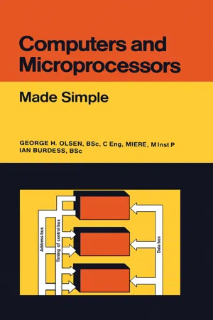 eBook - PDF
Computers and Microprocessors
Made Simple
- George H. Olsen, Ian Burdess(Authors)
- 2016(Publication Date)
- Made Simple(Publisher)
They are being used increasingly in consumer products, such as washing machines, sewing machines, toys and television games as well as scientific applications for data acquisition and control. This shift away from the traditional markets has, to a large extent, been due to the evolution and development of the basic Logic Gates used in their construction. Unlike analogue systems, the digital computer is constructed entirely of switching devices capable of assuming only two states, ON and OFF. As the demands for computers have grown and new markets have opened up, the semiconductor device manufacturers have responded by increasing the speed and reducing the size of the basic logic circuits. A majority of the systems in use today is now based upon the popular transistor-transistor logic (TTL) NAND gate. By using these TTL NAND gates, it is possible to design and construct a logic circuit capable of making decisions based upon the current state of the input signals. These combinational logic circuits may be used to perform such elementary tasks as checking the door interlocks of an automatic washing machine before the wash cycle starts, or they may be used to construct a com-plex and high-speed arithmetic unit of a computer capable of adding numbers together at the rate of hundreds of thousands per second. Combinational logic circuits are, however, incapable of learning by experi-ence and always respond to a given situation in exactly the same manner. Based upon the same TTL NAND gates, but by incorporating feedback, it is possible to construct a circuit which can take into account its past experience. These systems, referred to as sequential logic systems, are very important in computers as they can be used to store information and count events as they occur. Finally, at the centre of any computer is a unit which is capable of perform-ing arithmetic calculations at very high speed.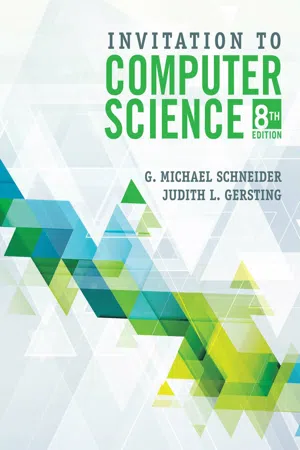 eBook - PDF
- G.Michael Schneider, Judith Gersting(Authors)
- 2018(Publication Date)
- Cengage Learning EMEA(Publisher)
This seemingly minor shift (from transistors to gates) has a profound effect on how computer hardware is designed and built. From this point on in our discussion of hardware design, we no longer need deal with anything electrical. Instead, our building blocks are AND, OR, and NOT gates, and our circuit construction rules are the rules of Boolean logic. This is another example of the importance of abstraction in computer science. George Boole was a mid-19th-century English mathematician, philosopher, and logician. He was the son of a shoemaker and had little formal education, having attended only elementary school. He taught himself mathematics and logic and mastered French, German, Italian, Latin, and Greek. He avidly stud-ied the works of the great Greek and Roman philosophers such as Aristotle, Plato, and Euclid. He built on their work in logic, argumentation, and reasoning and, in 1854, produced a book titled Introduction into the Laws of Thought . This seminal work attempted to apply the formal laws of algebra and arithmetic to the principles of logic. That is, it treated reasoning as simply another branch of mathematics containing operators, variables, and transformation rules. He created a new form of logic containing the values true and false and the operators AND, OR, and NOT. He also developed a set of rules describing how to interpret and manipulate expressions that contain these values. At the time of its development, the importance of this work was not apparent, and it languished in relative obscurity. However, 100 years later, Boole’s ideas became the theoretical framework underlying the design of all computer systems. In his honor, these true/false expressions became known as Boolean expressions , and this branch of mathematics is called Boolean logic or Boolean algebra . Even though he had very little formal schooling, Boole was eventually appointed professor of mathematics at Queens College in Cork, Ireland.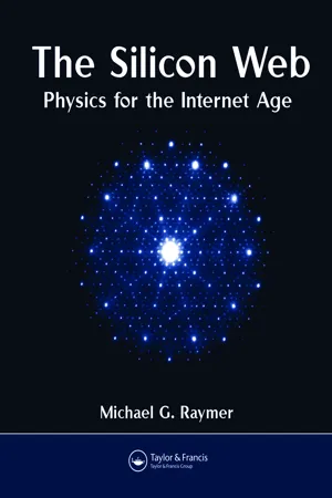 eBook - PDF
The Silicon Web
Physics for the Internet Age
- Michael G. Raymer(Author)
- 2009(Publication Date)
- CRC Press(Publisher)
A simple example occurs in a calculator when you press the “add” or “ + ” button. The input data are the two numbers you want to add (18, 5). The calculator carries out several logical operations to produce the resulting sum (18 + 5 = 23), which is the output data. Before we consider the actual electronic circuits that perform the operations, we will discuss the principles behind logic. English mathematician George Boole (1815–1864) was one of the founders of the principles of logic. In his honor, the methods used are called Boolean logic . In the context of modern computing, Claude Shannon was the most influential scientist who contributed to the theory of logic. In 1938, as a graduate student at Massachusetts Institute of Technology, he submitted his master’s thesis that showed how electronic circuits could be used to perform logic. Ten years later Shannon published the paper, “A Mathematical Theory of Communication,” which revolutionized scientists’ under-standing of the concept of information. 6.2 CONCEPTS OF LOGIC What is logic? In everyday life, it means to take in some information, apply certain rules of reasoning, and produce a decision. For example, you might reason that “if the sky is blue then I will take a walk without an umbrella, but if the sky is cloudy then I will take my umbrella.” The color of the sky is the input data and the umbrella decision is the output data. We can make a table showing our logic about the sky and umbrellas: Input: Sky blue? Output: Umbrella? No Yes Yes No The rules we use to process data or information are called logic operations . A logic operation is an elementary rule for arriving at a logical outcome. Three basic opera-tions that can serve as building blocks for all logic operations are NOT, AND, and OR. In considering complex situations, a diagram is useful to help visualize the logic process. Think of this as a flow chart for making a decision.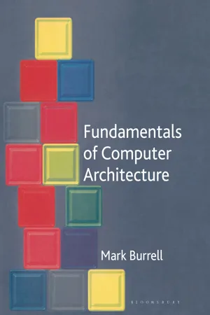 eBook - PDF
- Mark Burrell(Author)
- 2017(Publication Date)
- Red Globe Press(Publisher)
This will allow us to interact with our circuit; Click on input X, or more properly the interactive input button below the X symbol (as shown in figure 3.19) -you should find that the output S (shown connected to a simulated light emitting diode , or LED ) should light up. When the LED is lit, the output S is set to 1, and when it is clear, output S is set to 0 -in fact we can see the truth levels of all the wiring too as a 59 Fundamentals of Computer Architecture wire carrying a logical 1 is shown in black while a wire carrying a logical 0 is shown in grey. Try changing the inputs and see what the outputs change to -this should match completely the definition for this circuit in the truth table in figure 3.8. And that’s it! Figure 3.19 Our finished circuit in Digital Works, showing X = 1 60 Fundamental Concepts II -Digital Electronic Circuits CHAPTER SUMMARY Gate logic The fundamental gates are AND, OR and NOT. All other gates and circuits can be constructed from these; These gates model the logical operations AND, OR and NOT as we described in the previous chapter; Truth tables describe, given a set of inputs, the outputs for a given gate or circuit; Circuits can be built that model truth tables, by modelling the minterms with AND gates and feeding their outputs into an OR gate. Boolean algebra Named after George Boole, boolean algebra can be used to describe cir-cuits. The set of rules are known as the identities of boolean algebra, and most laws have two forms -an AND and an OR form; De Morgan’s laws can be used to make circuits more efficient by reducing the number of transistors used within a circuit. Using Digital Works Digital Works can be used to draw and then simulate logic circuits. SELF TEST QUESTIONS 1 Draw a circuit, using the methods described above, to meet the following truth table. R 0 0 0 0 1 1 1 1 X Y 1 0 0 1 2 Run the circuit in exampleschapter03assoc.dwm .
- J. David Irwin, David V. Kerns, Jr.(Authors)
- 2022(Publication Date)
- Wiley(Publisher)
CHAPTER 12 Digital Electronics and Logic Circuits LEARNING OBJECTIVES • To understand the binary number system • To learn to use Boolean algebra and its role in logic function minimization • To understand the types and operations of basic Logic Gates • To learn to realize NAND gates with both NMOS and CMOS devices • To learn to analyze and design combinational logic circuits • To learn to analyze and design sequential logic circuits INTRODUCTION Digital electronics is having, and will continue to have, a profound effect on vast areas of techno- logical development. In communications alone, the tentacles of this technology have permeated essentially every possible facet of this area. Only a cursory examination of the growth of cell phones around the world is sufficient to see the effect this technology is having on the lives of everyone. The Internet, which is a high-speed digital communication pipe, has made us aware of events all around the world in seconds of the time in which they have occurred. The processing speed of our computers, which is directly related to the advances in digital electronics, continues to increase at a phenomenal rate. Digital logic circuits, which form the backbone of the digital communication and processing systems, are driven by electronics that operate in a discrete mode. We saw in the last chapter that two of the transistor’s operating states are saturation and cutoff. While these operating states are not used in analog amplifiers, they are the building blocks for digital systems. In saturation, the output voltage of the transistor is low, and in cutoff the output voltage is high. We can then associate the high voltage with a logic state of 1 and the low voltage with a logic state of 0. The blazing speed of transistors permits us to shift from one state to another in the design of high-speed digital circuits. THE BINARY NUMBER SYSTEM The number of digits employed in any number system is called the base or radix. eBook - PDF
Mechatronics
A Foundation Course
- Clarence W. de Silva(Author)
- 2010(Publication Date)
- CRC Press(Publisher)
2. State the logic that connects the inputs and outputs and express it as a Boolean relation. 3. Minimize/optimize the relation. 4. Using the basic Logic Gates, sketch the realization that will satisfy the minimal Boolean relation. In a practical realization, it is important to minimize the cost and complexity. Accordingly, a minimal realization that uses the least number of basic gates would be preferred. This topic will be addressed under Karnaugh maps (K-maps). Also, it is desirable to use least number of types of Logic Gates (e.g., all NOR, all NAND). We now illustrate the design/ realization of combinational logic circuits for several practical applications. 8.4.3.1 Multiplexer Circuit A digital multiplexer selects one digital input channel from a group and connects it to the output channel (i.e., reads the input channel). Consider the case of a two-input multiplexer. The inputs are denoted by x and y . The output is a . The control signal for input selection is c . The logic function of the circuit may be expressed as follows: if 0 a x c = = if 1 a y c = = This logic may be translated into the following Boolean relation: a x c y c = ⋅ + ⋅ Its realization is shown in Figure 8.7. 8.4.3.2 Adder Circuits Logic Gates are used in the arithmetic and logic unit (ALU) of a microprocessor to perform various processing operations. A basic arithmetic operation that is performed by the ALU is addition . A simple logic circuit, which performs the addition of two binary digits (bits), is shown in Figure 8.8a. This is called a half adder . This circuit contains two OR gates, one AND gate, and one NOT gate. The added two digits are denoted by A and B (the inputs to the logic circuit). The sum of the two digits is denoted by S , and the carry to the next higher place is denoted by C . Clearly, the truth table given in Figure 8.8b agrees with the rules of binary addition of two bits.
Index pages curate the most relevant extracts from our library of academic textbooks. They’ve been created using an in-house natural language model (NLM), each adding context and meaning to key research topics.