Technology & Engineering
p type Semiconductor
A p-type semiconductor is a type of semiconductor material that has been doped with elements that introduce positively charged "holes" into the crystal lattice. This creates a surplus of positive charge carriers, which are responsible for the conduction of electric current in p-type semiconductors. When combined with n-type semiconductors, p-type semiconductors are used to create diodes and transistors in electronic devices.
Written by Perlego with AI-assistance
Related key terms
1 of 5
10 Key excerpts on "p type Semiconductor"
 eBook - PDF
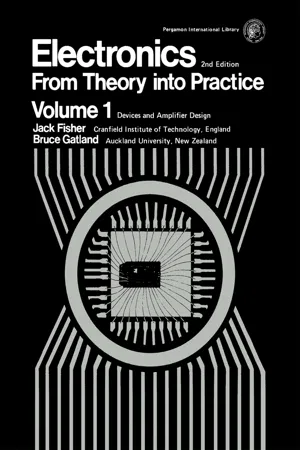
Electronics—From Theory Into Practice
Pergamon International Library of Science, Technology, Engineering and Social Studies
- J. E. Fisher, H. B. Gatland, P. Hammond(Authors)
- 2014(Publication Date)
- Pergamon(Publisher)
However, in this case an excess of holes will exist and these are the majority carriers. Since the majority carrier possesses positive charge such a material is known as p type. In the production of semiconductor devices, it is often required that the level of doping be controlled. The more heavily doped a material is, the lower is its resistivity. Heavily doped material is identified by the symbols n + and p + . 1 E.F.T.P. COMB—B 2 ELECTRONICS FROM THEORY INTO PRACTICE 1.1. The junction diode ' If a piece of semiconductor material is doped with p-type impurity at one end and n -type impurity at the other, then there will exist a junction between the two types. Some holes in the p region will diffuse into the n region leaving the p region slightly negative. Similarly, electrons from the n region will diffuse into the p region leaving the n region slightly positive. In a layer between the n and p regions, holes and electrons recombine and, since this layer is now depleted of free charge carriers, it is called the depletion layer. This layer acts as a potential barrier which opposes any further diffusion of charge, and the junction assumes a state of dynamic equilibrium. The condition is illustrated in Fig. 1.1a. I, mA Turnover voltage (constant) Reverse! bias f Forward bias (a) 1 ^ f Saturation | current (constant)| (b) Fig. 1.1. (a) Semiconductor junction showing the potential barrier caused by the diffusion of charge carriers. Under these conditions a potential exists between A and C. (b) Characteristic curve of a semiconductor diode. Note the change in current scale as the curve passes through the origin. If bias is applied to the terminals such that A is positive with respect to C, it has the effect of reducing the thickness of the depletion layer. The potential barrier is thus reduced and current will flow. eBook - PDF
Physics of Electronic Materials
Principles and Applications
- Jørgen Rammer(Author)
- 2017(Publication Date)
- Cambridge University Press(Publisher)
Two pieces of n-type and p-type semiconductor cannot just be glued together to form a functioning device, since if not carefully constructed there will be a myriad of electronic interface states, capturing charge, which would be detrimental to device functioning. Consider a semiconductor in which the impurity concentration is assumed to vary only along one direction. As an idealization, assume that in the left half-space of the semicon-ductor, z < 0, there are only acceptor impurities, and in the right half-space, z > 0, only donor impurities. The densities of donor and acceptor impurities are assumed constant, respectively n d and n a , and typically different. Understanding this simplified scenario then spells out the modifications to which a deviation from a sharp interface leads. 1 1 To have a rather sharp interface separating the n-type and p-type semiconductors is achievable by molecular beam epitaxy (MBE) technology, but certainly not by having dopants diffuse into the semiconductor crystal. Shooting in dopants using an accelerator also allows controlled dopant deposition by tuning the energy of the dopants. 249 250 Transistors Consider this contact of p-and n-type regions. At zero temperature, all the impurity elec-trons in the n-type material are bound in their hydrogen levels, and in the p-type material there are bound holes to the acceptor impurities, as depicted in Figure 11.1 , where only the acceptor and donor impurities in the region near the interface are depicted explicitly. For simplicity, the Bohr atomic orbital depiction of the bound impurity electron has been used instead of the proper wave function probability cloud of Figure 10.4 , and similarly a bound hole is depicted as in Figure 11.2 . On raising the temperature, the bound electrons in the n-type material are thermally excited to the conduction band of the semiconductor, and at room temperature they are all free carriers.
- Wei Gao, Nigel M Sammes;;;(Authors)
- 1999(Publication Date)
- WSPC(Publisher)
Thus, the electrons are the majority carriers and the holes are the minority carriers. 5.4.2. p-Type Extrinsic Semiconductors If trivalent impurities (B, Al, Ga and In) are substituted in the tetravalent lattice, the effect is the opposite of that described above. One of the four bands surrounding the impurity atom is missing one electron, leaving a hole in the valence band. If the hole moves away from the impurity atom, four saturated bonds and a net negative charge remain on the impurity atom. The hole is attracted to the charge and a set of quantum states is established (Figs. 5.7 and 5.8). The energy state of the hole is about 0.01 eV above the valence band. Thus, a hole can be created in the valence band merely by thermal excitation. This type of semiconductor is called the p-type extrinsic semiconductor. Semiconductor Properties and Materials 73 Fig. 5.7. An acceptor impurity in a semiconductor. (After Rose, Shepard and Wulff, Electronic Properties, John Wiley & Sons, 1966) Empty conduction Band Filled acceptor state Acceptor level Empty valence state: a hole In the valence band Fig. 5.8. Band structure for Fig. 5.7. (After Rose, Shepard and Wulff, Electronic Prop-erties, John Wiley & Sons, 1966) The energy level near the valence band attracting electrons from it is called the Acceptor level. The AE between the acceptor level and the va-lence band is equal to the binding energy between the hole and the acceptor atom. The liberation of the hole from the acceptor atoms is equivalent to the excitation of an electron from the valence band to the acceptor level. 74 An Introduction to Electronic and Ionic Materials In p-type extrinsic semiconductors, the majority carriers are holes and the minority carriers are electrons. 5.4.3. Doping In many intrinsic semiconductors, the impurity concentration is smaller than one part per million (1 ppm = 10 -6 = 0.0001%). eBook - PDF
- Geoff Lewis(Author)
- 2013(Publication Date)
- Newnes(Publisher)
The basic materials that are employed have a con-ductivity about halfway between that of conductors and insulators, hence the term semiconductor. These include: germanium (Ge), silicon (Si) and the Group III/V elements, aluminium (Al), gallium (Ga), indium (In) / arsenic (As), antimony (Sb) Semiconductor devices and technology 285 Germanium is now less used than silicon because of its poorer temperature characteristics (typical operating temperature 75°C compared with 200°C for silicon). 32.1 Behaviour of PN junctions Just as controlled conduction can be achieved through doping intrinsically pure tetravalent semiconductor elements (I type material) with trivalent or pentavalent impurities in a precisely controlled way, pseudo-semiconduction can be produced by the careful combination of the Group III (trivalent) and Group V (pentavalent) elements to produce a new class of device with even more useful characteristics. By adding pentavalent impurity atoms to I type material, addi-tional electrons are donated to the crystal structure. This forms an Ν type semiconductor material in which electrons form the majority current carriers. In a similar way, the addition of trivalent impurities leaves spaces or holes in the crystal structure which represent energy levels where electrons could exist. This Ρ type material thus has the positive charges of the holes as majority carriers. A hole therefore has an equal but opposite polarity charge to that of an electron. In both Ρ and Ν type materials there will always be some thermally generated charges of the opposite polarity and these are known as minority carriers. In certain applications, the Ρ and Ν type impurity layers may be doped to a relatively higher or lower level than normal. By convention, these regions would be indicated as P + or N + ; or P~ or N, respectively. eBook - PDF
- Behzad Razavi(Author)
- 2021(Publication Date)
- Wiley(Publisher)
As a result, the fourth bond contains a hole, ready to absorb a free electron. In other words, N boron atoms contribute N boron holes to the conduction of current in silicon. The structure in Fig. 2.6 therefore exemplifies a p-type semiconductor, providing holes as majority carriers. The boron atom is called an “acceptor” dopant. Si Si Si Si Si Si B Figure 2.6 Available hole with boron doping. Let us formulate our results thus far. If an intrinsic semiconductor is doped with a density of N D (≫ n i ) donor atoms per cubic centimeter, then the mobile charge densities are given by Majority Carriers: n ≈ N D (2.9) Minority Carriers: p ≈ n 2 i N D . (2.10) Similarly, for a density of N A (≫ n i ) acceptor atoms per cubic centimeter: Majority Carriers: p ≈ N A (2.11) Minority Carriers: n ≈ n 2 i N A . (2.12) Since typical doping densities fall in the range of 10 15 to 10 18 atoms∕cm 3 , the above expres- sions are quite accurate. Example 2-4 Is it possible to use other elements of Fig. 2.2 as semiconductors and dopants? Solution Yes, for example, some early diodes and transistors were based on germanium (Ge) rather than silicon. Also, arsenic (As) is another common dopant. Exercise Can carbon be used for this purpose? Figure 2.7 summarizes the concepts introduced in this section, illustrating the types of charge carriers and their densities in semiconductors. 28 Chapter 2 Basic Physics of Semiconductors Covalent Bond Si Si Si Electron Valence Intrinsic Semiconductor Extrinsic Semiconductor Silicon Crystal N D Donors/cm 3 Silicon Crystal N 3 A Acceptors/cm Free Majority Carrier Si Si Si Si Si Si P e n–Type Dopant (Donor) Si Si Si Si Si Si B Free Majority Carrier Dopant p-Type (Acceptor) Figure 2.7 Summary of charge carriers in silicon. 2.1.3 Transport of Carriers Having studied charge carriers and the concept of doping, we are ready to examine the movement of charge in semiconductors, i.e., the mechanisms leading to the flow of current. eBook - PDF
Electrons, Neutrons and Protons in Engineering
A Study of Engineering Materials and Processes Whose Characteristics May Be Explained by Considering the Behavior of Small Particles When Grouped Into Systems Such as Nuclei, Atoms, Gases, and Crystals
- J. R. Eaton(Author)
- 2013(Publication Date)
- Pergamon(Publisher)
As semiconductor devices have significant advantages over vacuum tubes in regard to both weight and space, they have aided appreciably in the minia-turization of electric circuits, particularly in such fields as hearing aids, aviation, communication equipment, and missile control systems. 18.2. T H E p-n J U N C T I O N The p-n junction consists of a single crystal of semiconductor material, such as silicon or germanium, which has almost perfect crystallographic structure throughout. The principle deviation from perfection is the result of intentionally added impurities whose distribution throughout the crystal is carefully con-trolled. The crystal, Fig. 18.1 (a), is grown in such a fashion that one section is p-type due to the fact that the concentration of acceptor atoms exceeds the con-centration of donors, while an adjacent section is «-type because of a preponder-ance of donor type impurities. The transition region between the two opposite types of impurity semiconductors is very thin, being of the order of a few lattice constants. The preparation of a crystal containing a p-n junction may be accomplished by several different methods. One is to grow a crystal from molten germanium to which a minute amount of acceptor impurity has been added. The crystal growth process is started by inserting into the molten material a small seed crystal which is continuously rotated and slowly withdrawn under proper tem-perature conditions. A crystal grows onto the seed forming />-type material. During the process of growth, donor type impurity is added to the melt in considerable quantity, the ensuing crystal growth being in the form of «-type material. After the crystal growth has been completed, a section may be cut out in the form of a wafer with the characteristics shown in Fig. 18.1. The produc-tion of crystals of uniform characteristics requires a high degree of refinement of chemical, metallurgical, thermal, and mechanical processes. eBook - PDF
Semiconductor Circuits
Theory, Design and Experiment
- J. R. Abrahams, G. J. Pridham, N. Hiller(Authors)
- 2013(Publication Date)
- Pergamon(Publisher)
No holes are pro-duced and conduction takes place by raising electrons from the = 5 = @ Hole available for conduction / Trivalent atom Valence electrons Ξ=#==·= Quadfavalent atoms Fio. 1.19. Covalent bonds in a p type Semiconductor. local donor level into the conduction band. The material is known as n type since the current flow is due to negatively charged electrons. In practice the donor level is 0Ό1 eV below the con-duction band for germanium and 0-054 eV for silicon and at normal temperatures the Fermi level may be regarded as lying between the conduction band and the donor level. The Fermi level does vary considerably with temperature and the reader is recommended to one of the many physics books available for a full treatment of this subject. In the case of a trivalent impurity such as boron, aluminium, gallium or indium, the three valence electrons form bonds, but one bond is left incomplete and gives rise to a hole. As in the case of an intrinsic semiconductor the application of an applied field BASIC PHYSICAL THEORY 23 causes the hole to move through the crystal lattice and conduction is by means of the positively charged holes. Free electrons are not produced in this process and the material is known as p type. This is shown in Fig. 1.19 while Fig. 1.20 shows the corresponding energy level diagram. The hole gives rise to a local empty energy level just above the valence band. Conduction is by means of hole movement at the top of the valence band, the local empty energy level readily accepting electrons from the valence band. The impurity energy level introduced is known as the acceptor energy FIG. 1.20. Energy levels in &p type Semiconductor. level E A and the Fermi level at normal temperature lies between the top of the valence band and the acceptor energy level. As in the case of donor impurities the reader is recommended to further reading on this subject. eBook - PDF
- Mircea S. Rogalski, Stuart B. Palmer(Authors)
- 2000(Publication Date)
- CRC Press(Publisher)
292 Solid State Physics 7.4. T h e p n J u n c tio n The pn junction, which is essential to the operation of most semiconductor devices and integrated circuits, consists of an abrupt discontinuity or a graded distribution of the two types of doping impurity across a region of a particular semiconductor sample. Although no surface states are involved in the boundary between the /7-type region and the n -type region, the electrostatic conditions at the junction can be obtained if we consider the special case where a piece of /7-type material is brought into intimate contact with a piece of zz-type material. The energy-band diagram at the moment of contact is given in Figure 7.10 (a). si V ( a ) ( b ) Figure 7.10. Energy-band diagram for an abrupt pn junction: (a) before contact (b) at thermal equilibrium Owing to the concentration gradient, electrons diffuse from the conduction band of the n-type region into that of the /7-type region and recombine with the free holes by dropping into the valence band. The space charge, produced by the negatively charged acceptors in the p-type side and the positively charged donors left behind in the n-type side, exerts a repulsive force on further charges crossing the junction, and inhibits further flow. In terms of the energy-band diagram, the Fermi energy of the /7-type region is raised with respect to that of the zz-type region until the Fermi levels become equal, as in Figure 7.10 (b), according to Eq.(7.57). The transferred charge which terminates on the immobile impurity atoms in the transition region produces an electric field which is directed from the n -type side to the p-type side. This built-in potential barrier Vint corresponds to the difference between the Fermi levels on the n and p sides before contact was made. eBook - ePub
Semiconductor Basics
A Qualitative, Non-mathematical Explanation of How Semiconductors Work and How They are Used
- George Domingo(Author)
- 2020(Publication Date)
- Wiley(Publisher)
Now there are empty spaces in the garage and cars can move from one empty space to another without the need to jump to the freeway. The boron impurities at room temperature leave a lot of empty spaces in the valence band and the electrons in the valence band can now move within the valence band. If I apply a positive voltage on the right, the electrons move to the right. The empty, parking, spaces move to the left and therefore it looks from the outside as if positive charges are moving to the left, i.e. to the negative terminal. As I mentioned before (see Section 2.4), we call these empty spaces holes and represent them by the letter p. The number of holes is almost identical to the number of indium atoms. Thus p ≈ N A, where N A is the density of acceptor atoms. I show this room temperature condition on the right of Figure 3.11. It is also important to emphasize that even though we talk about materials that have free electrons or free holes, the material itself is still electrically neutral. Sb has 51 electrons, five of them in the outer, valence, band but it also has 51 protons (positive charges) in the nucleus, therefore the material is electrically neutral (it also happens to have 71 neutrons which have no charge). Similarly, boron has five electrons, three of them in the valence band but it also has five protons and six neutrons in the nucleus, making it a neutral element. 3.6 Additional Considerations In both the n‐ and p‐type semiconductors I can change the electrical properties by adding impurities. Changing the number of free electrons or free holes also changes the resistivity of the semiconductors. Figure 3.12 shows the resistivity of n‐ and p‐type silicon at room temperature as the number of impurities I add to the silicon increases from 10 14 to 10 21 per cm 3. Notice that the scales are logarithmic scales. The resistivity changes by a factor of 1 million, from 0.0004 to 100 Ω‐cm eBook - ePub
Compact Models for Integrated Circuit Design
Conventional Transistors and Beyond
- Samar K. Saha(Author)
- 2018(Publication Date)
- CRC Press(Publisher)
Equation 2.65 , while the minority carrier electron concentration is given byn p≅n i 2N a(2.67) Since np ≪ p, electrons are minority carriers in a p-type semiconductor. Consequently, we often use the terminology of majority and minority carriers.From Equation 2.62 , we can write for an n-type semiconductor
where:ϕ i−ϕ f=lnk Tq(=)N dn ivlnk T(≡ −)N dn iϕ B(2.68) ϕB≡ (ϕf– ϕi) is called the bulk potential and is negative for n-type semiconductorsSimilarly, from Equation 2.63 , for p-type semiconductor, we can show
Thus, we can write a generalized expression for bulk potential in semiconductors asϕ f−ϕ i=vlnk T(≡)N an iϕ B(2.69)
where:ϕ B= (ϕ i−ϕ f) = ±vlnk T()N bn i(2.70) the “+” sign is for p-type semiconductors with Nb = Nathe “–” sign is for n-type semiconductors with Nb = NdNote that the Fermi potential, ϕf, is not only a function of carrier concentration but also dependent on temperature through ni . From Equation 2.70 , we observe that since ni increases with temperature according to Equation 2.15 , the magnitude of ϕBdecreases and as ni approaches to Nb , ϕfapproaches to ϕi
Index pages curate the most relevant extracts from our library of academic textbooks. They’ve been created using an in-house natural language model (NLM), each adding context and meaning to key research topics.