Physics
Semiconductor Devices
Semiconductor devices are electronic components made from semiconductor materials, such as silicon. They have the ability to control the flow of electrical current and are fundamental to the operation of electronic devices. Common semiconductor devices include diodes, transistors, and integrated circuits, which are essential for the functioning of modern electronics.
Written by Perlego with AI-assistance
Related key terms
1 of 5
9 Key excerpts on "Semiconductor Devices"
 eBook - PDF
- Fumio Shimura(Author)
- 2012(Publication Date)
- Academic Press(Publisher)
Chapter 4 Basic Semiconductor Physics Although this b o o k aims to provide comprehensive a n d up-to-date k n o w l -edge of the semiconductor silicon crystal technology, the ultimate objective of this effort is not only to contribute to the p r o d u c t i o n of state-of-the-art V L S I / U L S I devices but also to create future electronic devices on the basis of silicon materials. T o this end, u n d e r s t a n d i n g semiconductor physics is unquestionably helpful to the further use of silicon materials. In this chapter, the basic semiconductor physics considered to be essential to develop an understanding of semiconductor crystals is described. T h e subjects emphasized in this chapter include (1) electrical conductivity a n d (2) basic electronic-device operation physics. F o r detailed consideration of semiconductors a n d their device physics, the reader should consult the s t a n d a r d text b o o k s such as Refs. 1-5 listed at the end of this chapter. 4.1 Semiconductors 4.1.1 Properties of Semiconductors Definition of Semiconductor W h a t is a semiconductor? W h a t are its proper-ties? Although the term s e m i c o n d u c t o r is well k n o w n , it m a y n o t be easy to answer these questions quickly. A semiconductor is often defined simply from the viewpoint of electrical conductivity cr. T h a t is, semiconductors are materials with values of the electrical resistivity p (= 1/a) at r o o m tempera-ture generally in the range of ~ 1 0 ~ 2 to 1 0 9 Q c m , intermediate between conductors ( ~ 1 0 ~ 6 Q cm) a n d insulators ( ~ 1 0 4 to ~ 1 0 22 Q cm). Indeed, the term s e m i c o n d u c t o r is from such an electrical conductive characteristic. Electrical Properties A semiconductor has been defined as a material that has intermediate conductivity. However, a pure a n d perfect crystal of m o s t 82
- Dale R. Patrick, Stephen W. Fardo(Authors)
- 2020(Publication Date)
- River Publishers(Publisher)
Chapter 3 Semiconductor Devices INTRODUCTION Nearly any study of Semiconductor Devices begins with an investigation of atomic theory. This is purposely done to familiarize the reader with a number of ideas re- lated to semiconductor operation. Chapter 1 examined electrons, protons, and neutrons. Each of these parts had a specific role in the construction of an atom. Elements are classified according to the number of particles they possess. No two elements have the same physical struc- ture. OBJECTIVES Upon completion of this chapter, you will be able to: 1. Explain how Semiconductor Devices functionally operate. 2. Distinguish between conductors, semiconductors, and insulators. 3. Describe the crystal structure of representative semiconductor diodes and amplifying devices. 4. Describe the operation of devices in a circuit. 5. Be familiar with semiconductor device packaging and symbol representations. 6. Recognize the functional operation of diodes and amplifying Semiconductor Devices. 7. Describe how to test Semiconductor Devices and evaluate their status. 8. Describe forward and reverse bias characteristics of diodes. 9. Explain voltage-current characteristics of semicon- ductor devices. 10. Describe the operation of zener diodes, light-emit- ting diodes (LEDs), photovoltaic cells, photodi- odes, and varactor diodes. 11. Recognize NPN and PNP transistors. 12. Explain transistor biasing. 13. Describe transistor Alpha and Beta characteristics. 14. Explain the operation of JFET, MOSFET, and UJTs. SEMICONDUCTOR THEORY Chapter 1 pointed out that the electrons of a particu- lar atom are not an equal distance from the nucleus. They rotate in well-defined orbits. Each shell or orbit can hold only a certain number of electrons. Outer-shell electrons have a great deal to do with the electrical conductivity of an atom. Uncontrolled movement of these electrons causes certain atoms to be good electrical conductors. eBook - PDF
Semiconductor Circuits
Theory, Design and Experiment
- J. R. Abrahams, G. J. Pridham, N. Hiller(Authors)
- 2013(Publication Date)
- Pergamon(Publisher)
PART I Theory of Semiconductors A· This page intentionally left blank CHAPTER 1 Basic Physical Theory THE understanding of semiconductor diodes, transistors and the many other solid state devices that have been developed in the past decade involves a deeper knowledge of the physical structure matter than is required with the well-established valve circuits. In this chapter, the underlying physical principles will be developed and, in the next, applied to Semiconductor Devices. 1.1. The Atom The atom of any element is the smallest particle ofthat element capable of taking part in a chemical reaction. It may be regarded as being composed of electrons moving in circular or elliptical orbits about a relatively heavy nucleus of protons and neutrons as shown in Fig. 1.1. This model of the atom was proposed by Bohr in 1913 and although it has been displaced by later models for many purposes it is a convenient representation to show the action of Semiconductor Devices. Electrons have a mass of 9x 10 31 kg and carry a charge of 1-6 x 10 19 C, while protons have an equal positive charge but a mass 1838 times as great. Neutrons are about the same mass as protons but carry no charge. All atoms are about the same size, approximately 10 10 m in diameter, while the nucleus is about 10~ 15 m in diameter. The nuclei of the heavier elements provide a greater attractive force on the orbital electrons and constrict the electrons within approxi-mately the same atomic volume. The atomic number of an element is decided by the number of protons in the nucleus while 3 4 SEMICONDUCTOR CIRCUITS the atomic weight is governed by the number of protons and neutrons. 1.2. Electron Orbits The position and shape of the electron orbits were derived by Bohr who applied Planck's Quantum Theory to atomic structure. eBook - PDF
- Michael R Fisch(Author)
- 2004(Publication Date)
- WSPC(Publisher)
Chapter 1 1 Semiconductors 11.1 Overview Almost all common electronic devices use semiconductors. Yet, many read- ers might not be able to answer the question, “What is a semiconductor?” Similarly, they might not know the most basic science and technology of this important class of materials. In the spirit of trying to build understanding from the basics, this chapter introduces the reader to semiconductors. The basic question, “What is a semiconductor?” will be addressed first. In practice, pure semiconductors are not as technologically useful as “doped semiconductors,” semiconductors containing controlled amounts of impuri- ties. Thus, we will ask: (1) What is a semiconductor? (2) What is a doped semiconductor? (3) How are semiconductors doped? (4) Why are semiconductors doped? (5) How are semiconductors used to make electronic devices? (6) What are some electronic devices? (7) How do Semiconductor Devices work? 11.2 Introduction Semiconductors are of great importance to our everyday life. Almost every appliance, electronic entertainment device, and automobile contains semi- conductors, in the form of transistors, that are part of integrated circuits that are part of more complex systems. While the details of semiconductor technology are very complex, a basic understanding of what semiconduc- 189 190 LIQUID CRYSTALS, LAPTOPS AND LIFE tors are and how they are used is not too complex and is vitally important to our later understanding of the computer. The macroscopic behavior of semiconductors may be distinguished from metals and insulators in two ways. First, as the name implies, the (elec- trical) conductivity, or ability to conduct electricity, at room temperature is between that of metals (much higher electrical conductivity) and insula- tors (much lower conductivity). It is important to realize that this range of conductivity is quite large.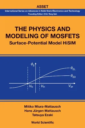 eBook - PDF
Physics And Modeling Of Mosfets, The: Surface-potential Model Hisim
Surface-Potential Model HiSIM
- Tatsuya Ezaki, Hans Jurgen Mattausch, Mitiko Miura-mattausch(Authors)
- 2008(Publication Date)
- World Scientific(Publisher)
Chapter 1 Semiconductor Device Physics 1.1 Band Structure Concept 1.1.1 Energy Bands and Quasi Particles The electronic properties of Semiconductor Devices are basically understood by quantum mechanics, since an electron is a quantum mechanical particle. One of the most important concepts for understanding the electric char-acteristics of Semiconductor Devices is the energy band structure which is composed of the electronic states from many atoms (i.e. 10 23 cm -3 ). The mechanisms, when the band structures are formed, can be explained only by quantum mechanics. Once we know the energy bands, the electrons in a semiconductor can be treated as “quasi” particles with properties similar to those of the classical particles, and we don’t have to get back explicitly to quantum mechanics any more. Thanks to this feature we can then easily capture device characteristics within the framework of classical mechanics and electro dynamics. In this section, the energy band structures of semi-conductor materials are briefly explained based on the quantum mechanical background. We first discuss the electronic states of isolated atoms. Table 1.1 shows the electron configurations of atoms from hydrogen to argon. Quantum mechanics tells us that the possible energy states of electrons in atoms are discretized, or quantized, because otherwise electrons would continuously lose parts of their energy by emitting electromagnetic waves, and would be sucked into the atomic nucleus. Quantized electronic energy levels under the central electrical force field of an atomic nucleus are classified as s , p , d , · · · orbitals according to the spatial probability distribution of the electron as denoted by the principle quantization number. This is listed in Table 1.1. Tables 162.1 and 162.2 in [5] give more complete data. See 1 2 The Physics and Modeling of MOSFETs Table 1.1 Electron configurations of atoms. eBook - PDF
- Stephen Thornton, Andrew Rex, Carol Hood, , Stephen Thornton, Stephen Thornton, Andrew Rex, Carol Hood(Authors)
- 2020(Publication Date)
- Cengage Learning EMEA(Publisher)
You will see how it is possible to understand the behavior of semiconductors by using the quantum theory of solids. We in- tend to present just enough of the theory in descriptive fashion to allow you to appreciate the versatility and importance of semiconductor materials. 11.1 Band Theory of Solids In Chapter 10 you learned about structural, thermal, and magnetic properties of solids. Here we concentrate on electrical conduction. There are three categories of solids, based on their conducting properties: conductors, semiconductors, and insulators. As seen in Table 11.1, the electrical conductivity at room temperature is quite different for each of these three kinds of solids. Semiconductor Theory and Devices 11 Copyright 2021 Cengage Learning. All Rights Reserved. May not be copied, scanned, or duplicated, in whole or in part. Due to electronic rights, some third party content may be suppressed from the eBook and/or eChapter(s). Editorial review has deemed that any suppressed content does not materially affect the overall learning experience. Cengage Learning reserves the right to remove additional content at any time if subsequent rights restrictions require it. 398 Chapter 11 Semiconductor Theory and Devices Metals and alloys have the highest conductivities, followed by semiconductors, and then insulators. We have already modeled the electrical conductivity of or- dinary metals in Section 9.6. The free-electron model used in Chapter 9 does not apply to semiconduc- tors and insulators. In fact there is a different conduction mechanism for semi- conductors than for metals. Striking evidence of this fact is seen in the resistivity- versus-temperature graphs presented in Figure 11.1. Although the free-electron theory correctly predicts a linear increase in resistivity with temperature, semi- conductors generally exhibit decreasing resistivity with increasing temperature. eBook - PDF
- Md Nazoor Khan, Simanchala Panigrahi(Authors)
- 2017(Publication Date)
- Cambridge University Press(Publisher)
The energy band diagrams of insulators have already been discussed in chapter 11. 430 Principles of Engineering Physics 2 12.2 Semiconductors Generally, the term semiconductor is applied to a class of materials having conductivity in between a conductor and an insulator. The forbidden energy band in semiconductors lies roughly in between 0.2 eV to 2.5 eV. Germanium and silicon are basic semiconductors. Early stage semiconductor electronic devices made of germanium have been replaced by silicon. Semiconductors possess the following characteristic properties: i. A pure semiconductor has a negative temperature coefficient of resistance [resistance decreases with increase in temperature] ii. Semiconductors give high thermoelectric power with signs both positive and negative relative to a given metal. iii. The junction between a p -type semiconductor and an n -type semiconductor shows rectification properties. iv. Semiconductors are light sensitive, generating either a photo-voltage or a change in resistance upon irradiation by visible radiation. 12.3 Band Theory of Semiconductors The band diagram of silicon and diamond are very much similar and has already been shown in Fig. 11.7. The atoms are so arranged that in diamond, the forbidden energy band is ª 7 eV and in silicon, it is only ª 1 eV. In case of a semiconductor, at room temperature, a small number of valence band electrons gain sufficient energy and jump to the conduction band. The energy band diagram of a semiconductor at 0K and at room temperature is shown in Fig. 12.1. Figure 12.1 Energy band diagram of a semiconductor. (a) At 0 K, the valence band is completely filled and the conduction band is completely empty. (b) At room temperature, a small number of valence band electrons gain sufficient thermal energy and jump to the conduction band. Therefore, at room temperature, the conduction band is partially filled and the valence band is partially empty eBook - PDF
Transistors: From Crystals To Integrated Circuits
From Crystals to Integrated Circuits
- Michael E Levinshtein, Grigory S Simin, Minna M Perelman(Authors)
- 1998(Publication Date)
- World Scientific(Publisher)
Sometimes it is important for electrons and holes to perish in the device as soon as possible. It is often quite essential for the fast switching of Semiconductor Devices. Then impurities creating effective recombination centres should be incorporated into the material. Sometimes, on the contrary, electrons and holes must live long. In this case, the semiconductor is to be thoroughly purified. 1.4 Summary Semiconductors are such materials whose conductivity at the temperature of absolute zero is equal to zero, all valence electrons being bound in the inter-atomic orbits and thus unable to conduct an electric current. The energy of the electron bonds is not very great, and even when the temperature is not high, the electron bonds break down on account of thermal motion. There appear free electrons (conduction electrons) and holes. Their concentration increases exponentially with the increase of temperature. And accordingly with the rise of temperature, the conductivity of semiconductors increases exponentially too. Some impurities (donors) are able to give away their electrons quite easily, while others (acceptors) can take electrons from the semiconductor atoms. Introducing such impurities, shallow impurities, even in very small quantities, may increase the number of free carriers to a very great extent and thus greatly increase the semiconductor conductivity. Chapter 1. The Main Properties of Semiconductors 37 Introducing into a semiconductor deep levels with a great ionization energy AE increases both the generation rate and the recombination rate of electrons and holes. With AE ss E g /2 the increase of the rates of generation and recombination is especially great. The influence of the deep levels is especially strong in non-equilibrium situations. When the concentration of electrons and holes is greater than under the equilibrium conditions, the presence of deep centres is displayed by an abrupt decrease of the lifetime of non-equilibrium carriers r. eBook - PDF
- D. Sands(Author)
- 2004(Publication Date)
- CRC Press(Publisher)
Chapter 2 Essential semiconductor physics The last chapter dealt very briefly with the origins of the diode laser. Although none of the physics was discussed in detail it was established that the laser was fabricated from a p-n junction. It is the purpose of this chapter to describe some of the essential concepts involved in the operation of such a junction; what do the designation n-type and p-type mean? how do electrons flow in such a structure, and how is light generated? The chapter is far from comprehensive. It is intended instead to provide a background from which the study of diode lasers can begin, and other concepts will come into play as the book progresses. It is certainly not the intention here to write a text book on semiconductor theory, as there are plenty of those you can consult [1-3] if you feel the need for a more thorough or more rigorous understanding of the topics raised here. The emphasis is placed firmly on the physics rather than the mathematics, but that does not mean that mathematics is not important. Some of the detailed concepts that arise throughout this book can only be understood properly in the light of the mathematical theories, but without a firm grasp of the physical basis for such theories much of the mathematics will be meaningless. 2.1 Free electrons in semiconductors Semiconductors, as the term implies, lie somewhere between insulators and metallic conductors, and chemical bonding plays a part in this. In metals the atoms pack together as closely as possible, the most common form being hexagonal close-packed structure. In order to do this the valence electrons from each atom are given up to a general pool of electrons and metals exhibit very high electrical conductivity as a result. In insulators, on the other hand, the electrons tend to be bound tightly to one or other of the constituent atoms, and so require the input of a large amount of energy to overcome the strength of the bond.
Index pages curate the most relevant extracts from our library of academic textbooks. They’ve been created using an in-house natural language model (NLM), each adding context and meaning to key research topics.